President Lee: “Mega-projects go beyond a race for speed to an all-out blitz” ... Samsung to invest 144 trillion won in Chungcheong region
- Input
- 2026-11-12 15:22:12
- Updated
- 2026-11-12 17:51:01
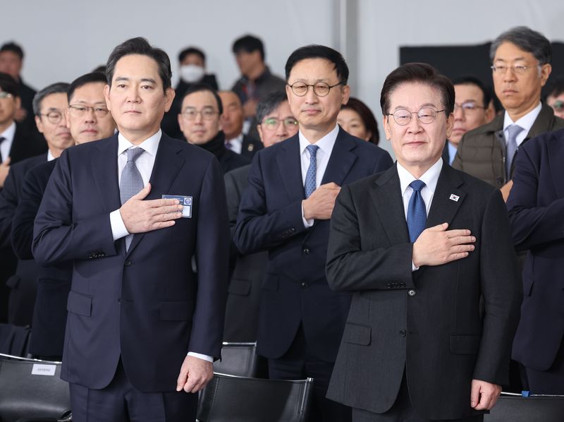
[Financial News] President Lee Jae Myung said on the 12th, regarding the megaprojects, that “execution, not promises, is what matters,” and called for support to ensure that investment by large corporations spreads throughout the region’s industrial ecosystem. Samsung will invest a total of 144 trillion won in the Chungcheong region to establish advanced industry hubs for high-bandwidth memory (HBM), organic light-emitting diodes (OLEDs), semiconductor package substrates, batteries and more.
■ President Lee: “Execution, not promises, is what matters”
At the fourth public-private joint review meeting on the megaprojects, held after the groundbreaking ceremony for the Chungcheong region megaproject at Samsung Electronics’ Onyang Campus in Asan, South Chungcheong Province, President Lee said, “For about four months since the megaprojects were announced, the government and businesses have been engaged in an all-out blitz, going beyond a race for speed, and changes are increasingly becoming visible on the ground.”In the Chungcheong region, six of the eight companies investing have begun making investments in earnest. In addition to the 392 trillion won in investment originally planned, 112 companies in fields including semiconductors and biotechnology are set to make additional investments totaling 23.6 trillion won.
President Lee said, “The megaprojects are not stopping at investment by large corporations. They are becoming a catalyst for technological innovation and investment at small and mid-sized companies and mid-sized partner firms, spreading throughout the industrial and regional ecosystems,” calling this “a very positive sign.”
He also called for support to help local SMEs enter new supply chains and to assist partner companies with financing and upgrading their manufacturing capabilities. He urged expanding opportunities for startups to demonstrate and commercialize their technologies, and called on local governments to provide housing, transportation, cultural amenities and other conditions that allow workers and their families to settle in the region.
President Lee stressed, “What matters now is action, not words. Execution, not promises, is what matters,” adding, “The promised and planned investment projects need to break ground and proceed on schedule for people in the region to have hope that their lives will really improve.”
The hope that the megaprojects would lead to jobs for young people in the region and changes in their lives was also evident at the groundbreaking ceremony that day. When a Chungnam National University student sharing the aspirations of Chungcheong’s young people said they had received an opportunity to interview with Samsung Electronics and remarked, “Being able to come in person to a Samsung Electronics site today makes that opportunity feel all the more meaningful,” President Lee, Chairman Lee and the other attendees smiled broadly.
■ Lee Jae-yong: “Transforming into a cutting-edge HBM hub for AI semiconductors”
Samsung’s investment plan for the Chungcheong region, announced that day, totals 144 trillion won: 60 trillion won from Samsung Electronics, 67 trillion won from Samsung Display Co., Ltd., 8 trillion won from Samsung Electro-Mechanics and 9 trillion won from Samsung SDI Co., Ltd. Samsung Electronics will invest a total of 60 trillion won in the Chungcheong region, including in Line 5 at its Onyang Campus. Foundation work is underway for Onyang Line 5, which is targeted to begin operations in June 2028, a year earlier than originally planned. The plan is to expand advanced packaging production capacity for next-generation HBM and boost the Chungcheong region’s semiconductor competitiveness by linking Onyang and Cheonan.In his welcoming remarks, Samsung Electronics Chairman Lee Jae-yong said, “Until just 40 years ago, all you could see from where you are standing was barren hills and unpaved roads. Now it has become an advanced factory that assembles and inspects semiconductors—the rice of industry—and completes them as finished products. With today’s groundbreaking ceremony, we pledge another leap forward. This site, once centered on processes that simply assembled and inspected conventional semiconductors, will transform into a cutting-edge HBM hub, the heart of AI semiconductors.”
Samsung Display Co., Ltd.’s 67 trillion won investment will be made in the Asan and Cheonan areas. The A7 line, construction on which began last month, is targeted to begin mass production in the second half of 2029, producing OLEDs for foldable devices, laptops and tablets.
In Sejong City, Samsung Electro-Mechanics will invest 8 trillion won to expand production capacity for advanced semiconductor package substrates for AI. It moved up the start of construction on a new plant to meet supply requests from big tech customers. After construction that began last month, mass production is expected to start in September 2028.
Samsung SDI Co., Ltd.’s Cheonan site will be developed as a “mother factory” for developing core battery technologies. The investment totals 9 trillion won. Construction was completed in July last year, and equipment began operating in November. Additional equipment is now being brought in. This expansion of investment is also expected to lead to further investments by partner companies.
The 194 partner companies that have grown alongside Samsung plan to invest approximately 18.1 trillion won in South Korea by 2030. SK hynix is introducing an “R&D Challenge Reward Program” that supports bold research and development regardless of whether it succeeds. By next May, it will also establish Trinity Fab, an environment similar to actual mass-production conditions, to support technology development and commercialization by materials, parts and equipment companies.
Meanwhile, after the fourth megaproject review meeting, President Lee had lunch with Chairman Lee and employee representatives in the cafeteria at Samsung Electronics’ Onyang Campus. Before the meal, Chairman Lee expressed his gratitude, saying, “We dramatically shortened what would have taken at least eight months and held today’s groundbreaking ceremony. With the President personally overseeing Gwangju, things look likely to move even faster.” Cheong Wa Dae spokesperson Kim Seong-wan said President Lee also praised Samsung’s bold investment decision and its ability to execute.
President Lee showed particular interest in how high school graduates develop into skilled technicians. When Kim Ju-woo, an employee on Samsung Electronics’ Yield Stabilization Team seated across from him, introduced themself as the first master technician in the HBM mass-production field, Chairman Lee explained, “Samsung has many employees who graduated from high school, and anyone can become a master technician after working for 20 years or more.”
President Lee then asked, “So high school graduates can become master technicians too?” Kim replied, “High school graduates from Meister high schools do their jobs well and are good at using AI, too.”
When a Samsung official explained that the company was struggling with a shortage of skilled pipefitters at construction sites, President Lee instructed Chief of Staff Im Gwang-hyeon to draw up a plan to train specialized piping workers.
[email protected] Choi Jong-geun Reporter