President Lee and Lee Jae-yong break ground on the first Chungcheong mega-project: “All investments to proceed without a hitch”
- Input
- 2026-11-12 15:22:07
- Updated
- 2026-11-12 15:49:32
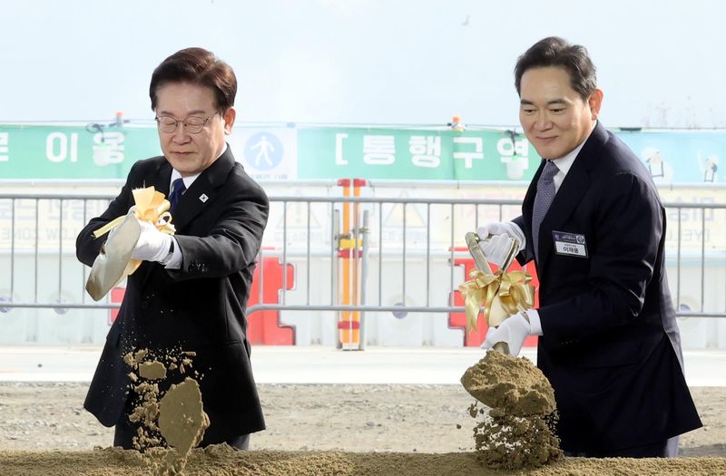
[Financial News] President Lee Jae Myung and Samsung Electronics Chairman Lee Jae-yong broke ground on the Chungcheong mega-project on the 12th. Its investment plan was announced last July. President Lee personally attended the first groundbreaking ceremony since the announcement of the three mega-projects last June. He promised, “To ensure that all investment plans—not only in Chungcheong but also in Honam and Yeongnam—proceed without a hitch, the central and local governments will work as one team and take clear responsibility through to the end for the various permits and approvals and for building key infrastructure such as power and water supply.” Lee Jae-yong also responded, “We will actively pursue the mega-projects in Honam and Yeongnam as well as Chungcheong.”
Speaking at the groundbreaking ceremony for the Chungcheong mega-project, held that day at the construction site of Samsung Electronics’ Onyang Campus in Asan, South Chungcheong Province, President Lee said, “Today, here in Chungcheong, we have energetically broken ground on three advanced investment projects that will reshape South Korea’s industrial landscape.”
He continued, “Last July, businesses and the government made a promise to the people right here in Chungcheong: an ambitious investment plan to make the country an industrial powerhouse with an unassailable technological lead. Just four months later, we are standing at the site where that promise is becoming reality.”
The ceremony was held to mark the full-scale launch of three advanced investment projects: an advanced semiconductor packaging fab and an advanced display production line in Asan, and a high-performance substrate manufacturing facility for AI servers in Sejong City.
Unlike usual, Lee Jae-yong greeted President Lee in front of the venue without wearing glasses. After delivering his congratulatory remarks, President Lee shook hands and spoke with Lee Jae-yong. The chairman, who had risen from his seat and was waiting, bowed again in greeting. The two were also seen exchanging words several times during the event.
The two then joined key attendees in taking up shovels and turning soil to mark the groundbreaking. President Lee said, “I am deeply grateful to Samsung Group executives and employees, including Chairman Lee Jae-yong, who made the decision to invest boldly and demonstrated swift execution, as well as to the residents of Chungcheong’s cities and provinces who joined forces to make today’s groundbreaking possible.”
He also personally outlined the investment plan for the Onyang Campus. President Lee explained, “This investment will establish a state-of-the-art packaging fab worth 6 trillion won, followed by additional investment totaling 40 trillion won in advanced equipment, rolled out in stages. The campus will grow into a key hub for advanced HBM (high-bandwidth memory) packaging.”
He added, “This wave of innovation is spreading rapidly throughout the Chungcheong region, beyond Asan and Sejong City. Preparations for groundbreaking are also proceeding without a hitch for memory and advanced packaging fabs in Cheongju, an artificial intelligence data center in Dangjin, and a biopharmaceutical production facility in Osong.”
[email protected] Choi Jong-geun Reporter