Taiwan Semiconductor Manufacturing Company Limited (TSMC): “Kumamoto Phase 2 to Use 3-nm Process; Japan Still Leads in the Semiconductor Ecosystem”
- Input
- 2026-11-11 15:09:11
- Updated
- 2026-11-11 15:09:11
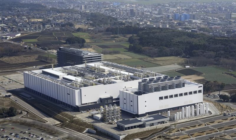
【Financial News, Tokyo—Correspondent Seo Hye-jin】Taiwan Semiconductor Manufacturing Company Limited (TSMC), the world’s largest foundry (contract chipmaker), said it plans to introduce a 3-nanometer (nm, one-billionth of a meter) process in the second phase of its expansion of its production base in Kumamoto, Japan. It also plans to meet demand in the physical artificial intelligence (AI) market through its partnership with Sony.
TSMC Senior Vice President Kevin Zhang said on the 11th at the World Management Meeting, hosted by The Nikkei and Switzerland’s International Institute for Management Development (IMD), “The Kumamoto site is expanding, and Phase 2 will use 3-nanometer technology.”
Zhang said TSMC’s first factory in Kumamoto was operating at full capacity and that the company was working with Sony, Japan’s leading image sensor company.
He said, “We will establish a joint venture (JV) with Sony to produce image sensors for future physical AI,” and stressed, “We are building production bases in this way to meet local demand.”
He also praised the competitiveness of Japan’s semiconductor industry. “Advanced semiconductor technologies and materials originated in Japan,” Zhang said. “Japan remains a leader in the semiconductor ecosystem.” He added, “Cars are shifting from being centered on mechanics to being centered on electronics, and semiconductors are inside them. Japan’s adoption of advanced semiconductors will continue to grow, and we, too, want to grow alongside our Japanese partners.”
He also highlighted the rising demand for computing power as AI spreads. Zhang said demand for computing power had surged as the use of “agentic AI”—which plans and performs tasks on its own—had spread over the past nine months. He predicted that customers were using TSMC’s most advanced processes in AI products and would move to 2-nanometer processes in the future.
He noted, however, that when deciding whether to expand production capacity, companies must consider not only semiconductor demand but also the constraints surrounding data centers.
He said, “At first, the discussion was that AI data centers needed logic chips, but when we spoke with customers, we found various constraints involving power and substrates. We need to look at the entire ecosystem to decide what to do with our production capacity.”
He also stressed the importance of working with local communities to build advanced factories. Zhang said, “Advanced factories need land, water and electricity. The first thing we need to do is build relationships with local communities and work with local governments as well.”
[email protected] Seo Hye-jin Reporter