Seoul attracts German firm Henkel’s semiconductor materials R&D center; Henkel to invest 12.1 billion won by 2031
- Input
- 2026-11-09 13:00:00
- Updated
- 2026-11-09 13:00:00
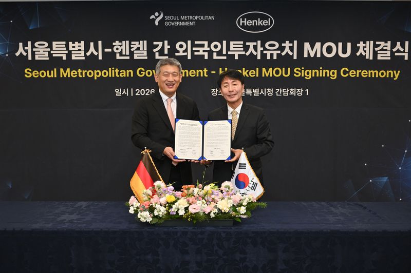
[Financial News] The Seoul Metropolitan Government has attracted an R&D center for next-generation semiconductor packaging materials from Henkel, a global German chemical company. Henkel plans to invest 12.1 billion won in Seoul by 2031 and hire 15 specialized research personnel.
The Seoul Metropolitan Government said it signed an MOU with Henkel on the 9th at the main building of Seoul City Hall to establish an R&D center for semiconductor packaging materials.
Under the agreement, Henkel will establish the Henkel Technology Center Korea, covering approximately 5,112 sq. m., at Gasan Digital Complex in Geumcheon District, Seoul. The company plans to consolidate its existing R&D functions in South Korea in Seoul while also setting up new R&D capabilities for advanced packaging materials needed for AI semiconductors and next-generation high-bandwidth memory (HBM). It plans to pursue foreign direct investment (FDI) totaling 12.1 billion won by 2031 and hire 15 research personnel, including people with master’s and doctoral degrees.
Founded in Germany in 1876, Henkel is a global adhesives, materials and consumer goods company operating in 79 countries worldwide. As of last year, it had annual sales of approximately 20.5 billion euros and around 50,000 employees. In South Korea, it operates manufacturing and R&D facilities through Henkel Korea, established in 1989, and has invested approximately 87.6 billion won to date.
The new R&D center will focus on developing advanced packaging technologies, including high-performance electronic adhesives and thermal management materials needed to improve the performance of AI and HBM semiconductors. Key research areas include liquid molding underfill materials that protect and secure semiconductor chips, heat-dissipation materials that remove heat generated by semiconductors, and bonding materials that enhance the structural stability of packages.
“South Korea is a key market leading the advanced semiconductor industry, backed by world-class semiconductor companies and outstanding technical talent,” said Jang Ho-jun, co-CEO of Henkel Korea. “Through this investment in the R&D center, we will strengthen our technological competitiveness in AI and HBM semiconductor packaging materials and expand our cooperation with the domestic semiconductor industry ecosystem.”
Henkel plans to expand materials development and joint research tailored to the technical needs of domestic semiconductor companies, leveraging its R&D center in Seoul. The Seoul Metropolitan Government will also support technology development and localization efforts for key materials, joint research with domestic companies that need them, and the development of young talent in partnership with universities and research institutions. It also plans to work with the central government to consider investment incentives under the Foreign Investment Promotion Act, helping ensure the smooth establishment of the R&D center and creation of new jobs.
“The attraction of Henkel’s R&D center is significant in that it will expand a global company’s advanced R&D capabilities in Seoul and could lead to technology cooperation with domestic semiconductor companies and the creation of quality research jobs,” said Kim Hyun-woo, head of the Seoul Metropolitan Government’s Economy Office. “We will continue to provide support so that Seoul can grow into a hub for advanced industry R&D and technological innovation.”
[email protected] Seong Cho-rong Reporter