[Exclusive] Samsung redraws its semiconductor investment map: Reconfiguring Giheung, its 'cradle,' and accelerating expansion in Pyeongtaek, Yongin and the U.S.
- Input
- 2026-11-04 18:07:25
- Updated
- 2026-11-04 18:07:25
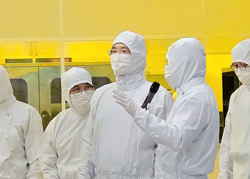
[Financial News] Analysts say Samsung Electronics' decision to center its plans for the Giheung site in Gyeonggi Province, the starting point of its semiconductor business, on a foundry (contract chip manufacturing) plant (fab) reflects the growing need for advanced production lines in South Korea to handle rising orders for artificial intelligence (AI) chips. Along with Giheung, Samsung Electronics is pursuing major expansions of its semiconductor production facilities in Pyeongtaek and Yongin. In the United States, the company plans to expand advanced foundry (contract chip manufacturing) facilities to meet rising demand for AI semiconductors.
■ Giheung, the 'starting point' of Samsung's semiconductor business, to become a foundry hub
According to semiconductor industry sources on the 4th, Samsung Electronics had been pursuing plans to build two research and office buildings on the former site of its Institute of Technology (SR5) at its Giheung facility in Gyeonggi Province. As demand for high-bandwidth memory (HBM) and server DRAM increased, there was speculation that a DRAM production line would be built there. But as the company reconsidered how to allocate research facilities and production lines on the limited site, it settled on making foundry the focus of 'Kairos,' a project to build new semiconductor production facilities.
The Giheung facility has played an important role in helping Samsung Electronics build its competitive edge in memory chip technology. Founded in 1987, the Institute of Technology (SR5) is a research facility that supported Samsung Electronics' development of the world's first 64-megabit (Mb) DRAM in 1992. As semiconductor production facilities later expanded to Hwaseong and Pyeongtaek, the Giheung facility came to focus on next-generation semiconductor research and development. Samsung Electronics began demolishing the SR5 and Samsung Electronics College of Engineering (CDI) buildings last September.
The decision to make foundry the initial purpose of the new semiconductor production facilities in this project is seen as reflecting the growing need to proactively expand advanced-process production capacity in South Korea as well. On its third-quarter earnings conference call this year, Samsung Electronics said demand for semiconductors used in AI and high-performance computing (HPC) was outpacing the pace of capacity expansion for leading-edge processes, and that it was increasing investment in new fabs at home and abroad.
Construction is also underway at the Giheung facility on NRD-K, a next-generation, integrated semiconductor research and development (R&D) complex. Samsung Electronics completed NRD-K's first research line and began operations in December 2024. The complex, which is being built on a site of about 109,000 square meters (33,000 pyeong), is expected to receive a total investment of 20 trillion won by 2030. NRD-K will conduct next-generation technology research and product development across all areas of semiconductors, including memory, System LSI and foundry. It will use advanced equipment, including high-resolution extreme ultraviolet (EUV) lithography systems and deposition equipment for new materials, to develop next-generation semiconductor processes and materials, and will also verify how research results can be applied to actual mass-production processes.
■ DRAM capacity expansion in Pyeongtaek; U.S. Taylor hub also growing
Samsung Electronics is designing 'Kairos' around foundry but has left open the possibility of converting it to a memory production line in the future. The company is increasing production capacity in Pyeongtaek for DRAM used in HBM, where demand is surging now. At Pyeongtaek Plant 4 (P4), it is expanding production lines for 10-nanometer-class sixth-generation (1c) DRAM used in HBM4. Pyeongtaek Plant 5 (P5) is also under construction, with its first fab targeted to begin operations in 2028 and its second in 2029.
Samsung Electronics is also expanding its production base in Yongin, Gyeonggi Province, and Taylor, Texas, in the United States. At the Yongin Advanced System Semiconductor National Industrial Complex being developed in the Cheoin District of Yongin, Gyeonggi Province, the company will invest about 360 trillion won to build six fabs in phases. The first production line is targeted to begin operations in October 2029.
In the United States, Samsung Electronics is building advanced foundry production facilities in Taylor, Texas. The first fab has begun operating its cleanroom and received its equipment, and work is underway to build out the production line. Samsung Electronics plans to break ground on a second fab this year and begin production in 2030. The Taylor plant is Samsung Electronics' U.S.-based advanced foundry hub, designed to produce semiconductors used in AI and high-performance computing (HPC), among other applications. The company is building production facilities centered on a 2-nanometer (nm; 1 nm = one-billionth of a meter) process and is also working to secure local customers.
A semiconductor industry official said, "Samsung Electronics is expanding memory and foundry production facilities together at key locations at home and abroad. With demand for AI semiconductors rising rapidly, securing a production base that can respond to market changes will determine the company's competitiveness going forward."
[email protected] Lim Su-bin, Park Ji-yeon Reporter