[Exclusive] Samsung’s ‘Kairos’ project in Giheung to focus on foundry production, with memory conversion also in view
- Input
- 2026-11-04 18:02:47
- Updated
- 2026-11-04 18:02:47
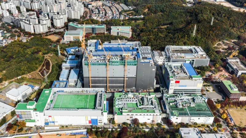
[Financial News] Samsung Electronics Co., Ltd. has decided to make foundry (contract semiconductor manufacturing) the focus of ‘Kairos,’ a project to build a new semiconductor facility at its Giheung site in Yongin, Gyeonggi Province, where the company’s semiconductor business began. The plan is also to develop Giheung, which laid the foundation for the growth of Samsung’s memory semiconductor business, into an advanced foundry production hub. The company will build a foundry plant first, while accounting from the initial design stage for the possibility of converting it into a memory production facility in the future, in a bid to respond to shifts in demand in the AI semiconductor market.
According to semiconductor industry sources on the 4th, Samsung Electronics is moving ahead in earnest with ‘Kairos,’ a project to build a new semiconductor facility at its Giheung site. Kairos is the name of a project related to the construction of new facilities, not an individual factory. Through the project, Samsung Electronics has decided to build the new semiconductor production facility as a foundry plant.
Samsung Electronics has recently been reviewing its medium- to long-term plans to expand facilities at its Giheung site and pursuing ways to strengthen both R&D and production. In particular, the company initially planned to build two buildings for a new R&D center on the site of the former General Technology Research Institute (SR5), but later changed course to develop a semiconductor production facility there. The new fab’s intended use was the subject of ongoing discussion, including the possibility of a DRAM production line or foundry operations, but the company ultimately decided to build it as a foundry production facility.
One notable feature is that, even as the fab is being built for foundry production, the possibility of converting it into a memory production facility in the future is being considered from the outset. Foundry and memory production differ in their processes and equipment configurations, so converting an actual production line would require additional investment in equipment and process adjustments. This suggests that the company is considering the facility’s long-term potential so its use can be changed depending on future market conditions and production strategies.
Construction related to the Kairos project is already underway following the decision on the facility’s use. Samsung E&A recently said it was carrying out structural work on the Kairos complex building, Green Building and substation at Samsung Electronics’ Giheung site.
The growth of the global AI semiconductor market lies behind Samsung Electronics’ broad consideration of how its new production facility could be used. Investment by big tech companies in AI data centers is driving a sharp increase in demand for high-bandwidth memory (HBM) and server DRAM, while competition to secure production capacity is also continuing in the advanced foundry market, which produces AI accelerators and other products.
The technological competitiveness of both fields is becoming increasingly important, particularly because AI semiconductors use high-performance memory alongside advanced logic semiconductors. Samsung Electronics, an integrated device manufacturer (IDM) with both memory and foundry businesses, is pursuing a strategy of expanding production capacity in line with market demand and customer investment plans. The Kairos project is also being pursued as part of this medium- to long-term semiconductor investment strategy.
This investment strategy is also tied to the changing role of the Giheung site. Samsung Electronics is expanding the site’s functions by developing Giheung into a next-generation semiconductor R&D hub while also adding new production facilities. A key example is its plan to invest approximately 20 trillion won in NRD-K, a next-generation semiconductor R&D complex, by 2030. NRD-K is a facility responsible for research into next-generation technologies and product development across all areas of semiconductors, including memory, System LSI and foundry. With the Kairos project also moving forward, the Giheung site is expected to expand its role as a hub combining advanced semiconductor R&D and production.
A semiconductor industry official said, “As the AI semiconductor market grows rapidly, decisions about investment timing and equipment configuration are becoming as important as securing new production facilities,” adding, “Given the nature of semiconductor fabs, which require large-scale investment, a strategy that takes medium- to long-term demand into account will determine future competitiveness.”
[email protected] Lim Su-bin, Park Ji-yeon Reporter