“Securing advanced AI packaging technology” — Lee Jae-yong inspects Japan’s future semiconductor packaging lab
- Input
- 2026-11-01 16:00:00
- Updated
- 2026-11-01 16:00:00
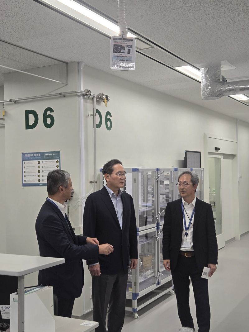
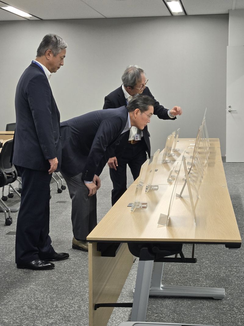
[Financial News] Samsung Electronics Chairman Lee Jae-yong visited an advanced semiconductor packaging research hub in Japan on the 1st to review progress in securing next-generation technologies. As competition in AI semiconductors expands beyond the performance of individual chips to packaging technology that connects multiple semiconductors, the move is aimed at boosting future competitiveness through cooperation with Japan’s materials, parts and equipment ecosystem.
After visiting a domestic advanced R&D complex and an HBM production line, as well as an overseas packaging research hub, Lee appears to be stepping up efforts to strengthen semiconductor competitiveness from next-generation technology development through mass production.
■Expanding ties with Japan’s materials, parts and equipment sector; focus on next-generation packaging
Samsung Electronics said Lee visited the Advanced Package Lab (APL) in Yokohama, Japan, that day. It was his first on-site inspection, about two months after the lab officially opened on September 8.After reviewing progress with researchers on the development of advanced packaging materials and process technologies and discussing ways to work with Japan’s materials, parts and equipment industry, Lee called for efforts to secure advanced packaging technologies.
Advanced packaging integrates various semiconductors, including graphics processing units (GPUs), HBM and accelerator chips, into a single package. It directly affects the bandwidth for data exchange between chips, power efficiency and heat management, and is emerging as a key area of competition in AI semiconductors.
Samsung Electronics established APL in Yokohama in 2023 as a research hub connecting its semiconductor design and manufacturing capabilities with the technological expertise of Japanese materials, parts and equipment companies. It officially opened the lab in early September after investing 40 billion yen (about 350 billion won) over five years starting in 2024.
APL’s main role is to develop and validate core technologies, including materials and processes required for advanced semiconductor packages. Going forward, it plans to expand its role beyond research into next-generation process and materials technologies to include developing new high-performance packaging structures needed for mass production of low-power, high-performance semiconductors.
Samsung Electronics plans to continue expanding its local research staff and develop APL into a global R&D hub. It also aims to boost R&D synergies in Korea and abroad through close collaboration with the packaging research unit under its Semiconductor Research Institute in Korea, while pursuing different research areas.
Samsung Electronics said, “Japan has many companies with world-class expertise in semiconductor materials, parts and equipment, and its industry-academia-research ecosystem is also well developed.” It added, “Above all, Yokohama is home to a concentration of companies supplying materials and equipment for advanced packaging, making it a suitable place to pursue joint research and technological cooperation.”
■Maintaining an unrivaled lead in semiconductors; reviewing technology and mass production
Lee’s visit is part of his on-site management spanning semiconductor facilities in Korea and abroad. After reviewing the foundation for next-generation technology development in Giheung and HBM back-end processes and quality in Cheonan, he checked progress in securing materials and processes for future packaging in Japan. The visit is seen as an effort to focus on securing an unrivaled lead in semiconductors by inspecting both the research infrastructure for developing future technologies and the production sites where they are put into practice.Lee visited the site of the NRD-K (New Research & Development - K) advanced semiconductor R&D complex under construction at Giheung Campus twice, in October 2023 and December 2025. He also inspected semiconductor production lines at Hwaseong Campus and elsewhere, reviewing technology development and manufacturing competitiveness.
NRD-K is a state-of-the-art integrated R&D complex covering about 33,000 pyeong, with total investment reaching 20 trillion won by 2030. It is being developed as a key hub for next-generation technology research and product development across the semiconductor sector, including memory, System LSI and foundry, with infrastructure planned to enable research results to move quickly into mass production.
Lee has also visited the Cheonan Plant in South Chungcheong Province, in February 2023 and this June, to review advanced packaging production and assess semiconductor back-end process capabilities.
The Cheonan Plant is a key production hub responsible for Samsung Electronics’ HBM back-end processes and advanced packaging. During his visit this year, Lee went to the cleanrooms at the C1 and C2 lines and inspected the HBM production lines.
[email protected] Kim Hak-jae Reporter