Samsung forms a semiconductor “Core Team” ... steps up its drive for an overwhelming technological lead
- Input
- 2026-10-21 18:36:19
- Updated
- 2026-10-21 18:36:19
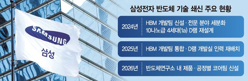
According to the semiconductor industry on the 21st, Samsung Electronics’ Device Solutions (DS) Division recently established “Core Teams” around major R&D projects within the Semiconductor Research Center and has begun operating them in earnest. The teams are reportedly organized across key technology fields, including DRAM, NAND and leading-edge foundry processes, and given “nicknames” based on the names of the related R&D projects.
The Semiconductor Research Center is under the chief technology officer (CTO) of the Device Solutions Division and is responsible for the pre-development of next-generation semiconductor technologies and processes. The Core Teams will focus on bringing together relevant personnel around key development projects for each product and improving the quality and speed of technology development through collaboration across organizations. The move is intended to pool development capabilities across fields within the center and strengthen collaboration throughout semiconductor development, from early-stage technology development and process design to packaging and mass production.
Samsung Electronics has previously operated an “One Team” system within the research center to research and develop leading-edge processes, as part of efforts to strengthen its competitiveness in the semiconductor business. Under the system, personnel are selected from memory, foundry and shared organizations to jointly develop key products, including high-bandwidth memory (HBM), next-generation DRAM and leading-edge foundry processes. The reorganization is seen as a move to form Core Teams, take the existing One Team system a step further and strengthen the execution of key technology development projects.
“Since the One Team system was introduced, tangible results have been emerging in leading-edge process areas that had been seen as lagging behind competitors such as SK hynix,” an industry source said. “The aim is to convert organizations that have so far operated in the form of task forces (TFs) into permanent teams, pool R&D capabilities and maximize synergies across organizations.”
As semiconductor processes become finer and product structures more complex, the technical challenges involved in R&D are increasing. For next-generation DRAM, securing yields during transitions to finer processes is considered a key challenge, while NAND processes are becoming more complex as more layers are stacked. In foundry technology, too, the ability to implement processes reliably determines competitiveness as the industry moves toward the most advanced nodes, including 2 nanometers (nm; 1 nm is one-billionth of a meter) and 1.4 nm. As a result, pooling R&D capabilities across fields such as process technology, design and materials—not just the technical expertise of individual organizations—is becoming increasingly important.
The reorganization is also understood to reflect an aim to strengthen the motivation of researchers involved in developing key technologies. At the Semiconductor Research Center, concerns have been raised that performance bonus criteria differ depending on an employee’s organization, even when they are working on the same development project. “I understand that some Core Teams receive performance bonuses at the level of the Memory Business Division if they meet their R&D project targets,” an internal source said. “The aim is to reflect key researchers’ contributions in their compensation, strengthen collaboration across organizations and boost the morale of development staff.”
[email protected] Im Su-bin Kim Jun-seok Reporter