Samsung’s Semiconductor Business Moves Beyond ‘One Team’ to ‘Core Teams,’ Betting on Elite Teams for Future Technologies
- Input
- 2026-10-21 16:39:34
- Updated
- 2026-10-21 16:39:34
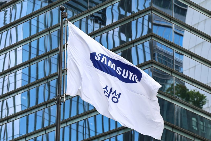
[Financial News]“Our performance fell short of market expectations, causing concern not only about our fundamental technological competitiveness but also about the company’s future. Achieving excellence in quality is the only way for Samsung Electronics to make a comeback.”This was the key message in the apology issued unusually by Jun Young-hyun, vice chairman and head of Samsung Electronics’ Device Solutions (DS) division, immediately after the company announced its preliminary third-quarter results in October 2024. At the time, Samsung Electronics was trailing in the High Bandwidth Memory (HBM) race and struggling to secure yields (the share of defect-free products) for advanced DRAM. It made restoring its fundamental technological competitiveness its top priority. The company then focused its resources on rebuilding its technological capabilities, including redesigning the DRAM that underpins HBM, reorganizing its HBM development teams and redeploying key personnel.
After posting record results in the third quarter of this year, Samsung Electronics is broadening its overhaul to include organizations for advanced research and development (R&D) into next-generation semiconductor technologies. Its recent establishment of a dedicated “Core Team” within the Semiconductor Research Center to develop key technologies is also part of an effort to secure leadership in the future semiconductor market. The company plans to strengthen its medium- to long-term competitiveness by bringing together specialists to develop leading-edge processes and foundational technologies in both memory and foundry (contract semiconductor manufacturing).■ Reclaiming a decisive edge in semiconductors: a sweeping overhaul starting with DRAMAccording to semiconductor industry sources on the 21st, Samsung Electronics recently established and began operating a “Core Team” within the Semiconductor Research Center dedicated to developing key next-generation technologies. The teams are organized around key products expected to determine future leadership in the semiconductor market, including next-generation DRAM (D1d), NAND flash (V12) and foundry processes at 2 nanometers (nm; one-billionth of a meter) or below. The company plans to bring together specialists from different fields—including memory, foundry and advanced packaging—according to each product’s development needs, strengthening collaboration between teams and improving the quality of its technology development.
The new organization is an extension of Samsung Electronics’ strategy to restore its technological competitiveness, which it has pursued for roughly two years. Since yielding its lead in the HBM market to SK hynix, the company has consistently operated dedicated teams and task forces (TFs) while reorganizing its development system.
Earlier, in July 2024, Samsung Electronics consolidated its previously dispersed development teams, established an HBM development team and organized its work around more specialized areas. It also launched a “One Team” system to strengthen collaboration between business divisions and tackle technical challenges, and took the major step of redesigning the product itself. Believing that the quality and performance of the DRAM underpinning HBM needed fundamental improvement, Vice Chairman Jun ordered a redesign of the 10-nanometer-class fourth-generation (1a) DRAM, identified as one of the obstacles to mass production of HBM3E.
The results subsequently began to emerge, including HBM3E passing quality qualification tests at major customers and expanded supplies. In November last year, Samsung Electronics integrated its separate HBM development team into the organization responsible for memory development and reassigned related personnel to the DRAM Development Office, stabilizing its development system.
As a result, this year Samsung Electronics became the first company in the world to supply HBM4 to NVIDIA Corporation, and went on to expand supply partnerships with global technology giants such as Advanced Micro Devices, Inc. (AMD). In the third quarter, buoyed by a semiconductor boom, its quarterly operating profit surpassed the 100 trillion won mark. Samsung Electronics is also accelerating development of next-generation DRAM processes to maintain this technological edge.
A task force dedicated to developing ultrafine DRAM processes below 10 nanometers—including 0a, the stage after 1d—is also operating within the Semiconductor Research Center. Alongside strengthening the technology of the foundational DRAM that determines HBM performance and power efficiency, the company is investing resources in developing next-generation NAND flash processes.■ Foundry also steps up development of leading-edge processesSamsung Electronics’ technology overhaul is expanding beyond memory into foundry as well. That is because the technological maturity of leading-edge processes and the ability to manufacture reliably at scale are key factors determining competitiveness in winning orders.
The Semiconductor Research Center is in fact operating a Core Team responsible for projects related to leading-edge foundry processes. It is focusing on stabilizing yields for the 2-nanometer process and securing customers, while also pursuing development of next-generation processes such as 1.4 nanometers. As the technical challenges of process miniaturization grow, the company is concentrating on bringing together key personnel from the early R&D stage to improve technological maturity.
Foundry in particular requires close collaboration across fields such as transistor structures, materials and design technology as processes become smaller. If technical challenges are not resolved during R&D, this can directly lead to delays in mass production and lower yields. Samsung Electronics’ move to bring specialists together for each key project is seen as a measure to reduce these risks and improve the efficiency of technology development.
An industry official said, “The success of advanced semiconductor development depends not only on the technological capabilities of individual teams but also on the level of collaboration across fields such as design and process engineering,” adding, “It will be important to see whether bringing together key researchers leads to tangible results not only in memory but also in non-memory sectors.”
[email protected] Im Su-bin, Kim Jun-seok Reporter