A giant expanded the playing field in a downturn ... laying the groundwork for an overwhelming semiconductor lead by overcoming a 1 trillion won risk [On the sixth anniversary of Lee Kun-hee: The visionary who shaped the future]
- Input
- 2026-10-20 18:26:51
- Updated
- 2026-10-20 18:26:51
Lee Kun-hee, Samsung’s late former chairman, was always focused on securing a competitive edge in the “next market” first. When competitors hesitated to invest, he changed production methods; when existing technologies neared their limits, he developed new structures. His strategy was to expand facilities while boldly widening the gap in technology, cost and mass-production capabilities.
As the center of the semiconductor industry shifts toward artificial intelligence (AI), the importance of management decisions that channel current results into investment in next-generation technologies is also growing. Lee’s foresight—he consistently moved several steps ahead of others—is now seen as a guide to management for the present day. There is broad agreement that his forward-looking leadership made a major contribution to Samsung Electronics Co., Ltd. gaining dominance in the global memory market in the AI era.
■ The gamble that risked a loss of 1 trillion won
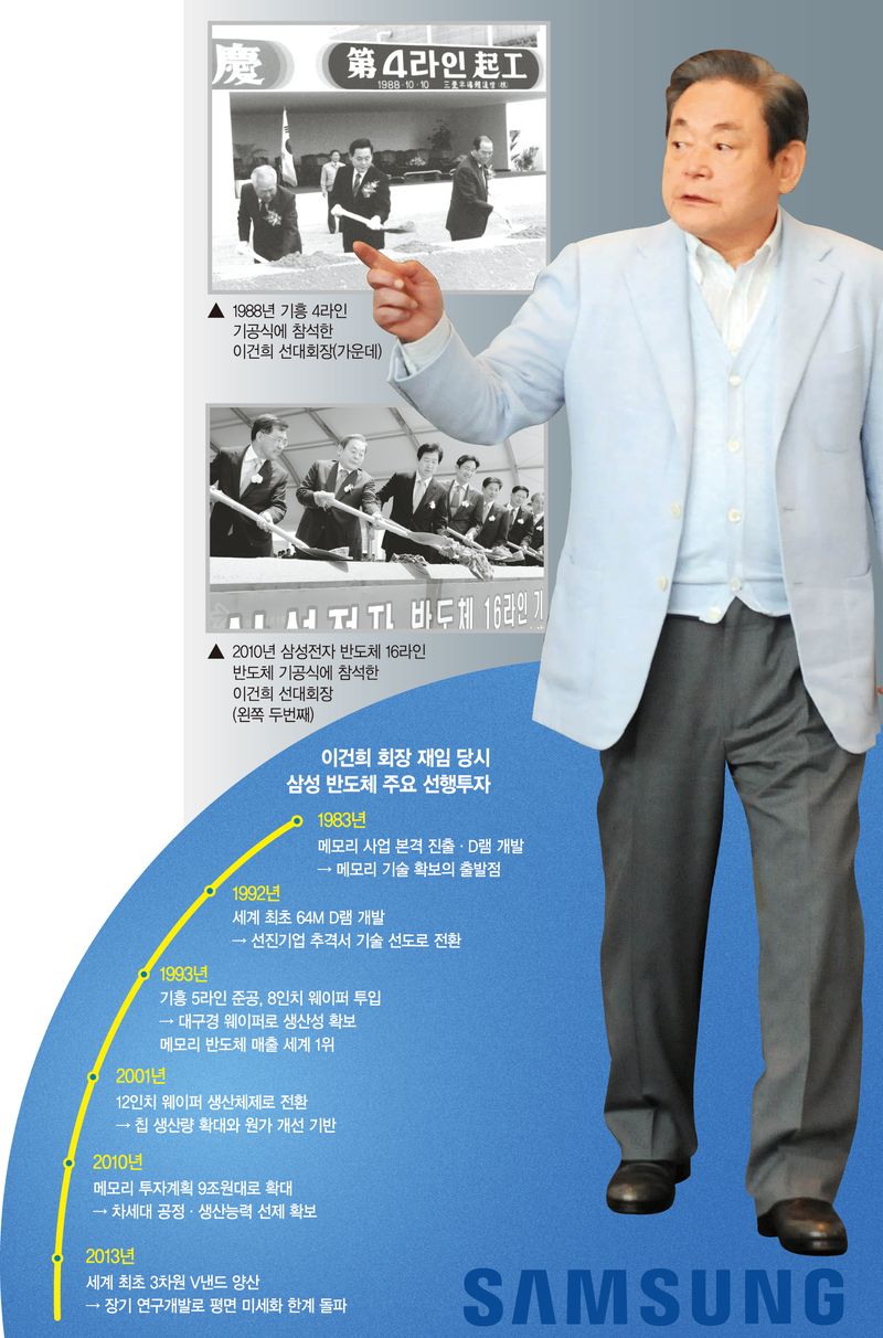
According to industry sources on the 20th, 12-inch (300 mm) wafers are now used primarily in Samsung Electronics’ advanced semiconductor production. Their wafer area is 2.25 times that of 8-inch (200 mm) wafers, making them advantageous for cost competitiveness. The foundation of this large-wafer production system lies in the early investment championed by Lee. The investment in 8-inch wafer production lines in the early 1990s was one of Lee’s signature gambles, transforming Samsung from a company that had only been playing catch-up. It meant choosing larger wafers than the 6-inch standard of the time so that more chips could be produced from each wafer. The risks were as great as the potential productivity gains: equipment and processes had to be changed, and yields—the proportion of usable products—had to be secured. In a 1997 essay, Lee recalled that the investment faced fierce opposition from those around him because a failure was expected to cause losses of more than 1 trillion won.
Nevertheless, Lee judged that it would be difficult to take the lead simply by following competitors’ successes. Believing Samsung could not afford to miss the accelerating pace of technological change, he pushed ahead with investment in 8-inch wafers in 1990–1991, during a downturn in the DRAM market. By expanding production from 6-inch to 8-inch wafers, Samsung gained an edge over Japanese rivals and rose to No. 1 in the world in memory semiconductor sales that same year.
Innovation did not stop at increasing wafer size. In 2013, while Lee was actively involved in management, Samsung began mass-producing the world’s first three-dimensional vertical-structure NAND flash memory.
Kim Yong-seok, a distinguished professor at Gachon University’s semiconductor college who worked at Samsung Electronics for 31 years, noted, “Lee Kun-hee understood that manufacturing capabilities are critically important in the equipment-intensive memory industry. His decision to expand production lines and investment during a downturn, thereby outpacing competitors, has important strategic significance.”
■ Lee Kun-hee’s forward-looking leadership
Lee Kun-hee’s leadership is considered significant because it always sought out the benchmarks for the next round of competition first. His leadership, which always kept the future in mind, is seen as a model even in the AI era, when companies must preserve their current advantage while securing the technology and talent needed for the next market.
In fact, Lee’s technology-driven management was not confined to semiconductors. From the time he took office in 1988, he foresaw a major transformation in the use of computers and predicted that advanced technologies such as semiconductors, computers and robots would determine future industrial competitiveness. He stressed that, alongside securing equipment, it was important to build the capability to use software.
The focus on future investment continued after the global financial crisis. In 2010, Samsung Electronics increased its memory investment plan from 5.5 trillion won to the 9 trillion won range. It planned to invest 12 trillion won in stages through completion of Line 16 in Hwaseong, and Lee urged the company to increase investment and hiring to secure global business opportunities ahead of its competitors. That year, actual spending on semiconductor facilities reached 12.7 trillion won.
As the integration of memory, processing units and software becomes increasingly important in the AI era, the industry continues to look to Lee Kun-hee’s leadership for guidance. Investments to improve semiconductor performance must go hand in hand with the ability to identify new markets for their applications.
Hwang Yong-sik, a professor in the Department of Economics at Sejong University, said, “Through his management, Chairman Lee Kun-hee identified the niches in the memory business and took a strategic approach. Rather than entering a red ocean unnecessarily, fighting fiercely and coming away with nothing but wounds, companies should use thorough market and industry-structure analysis to find fields that offer sufficient investment value and strong prospects.”
[email protected] Kim Hak-jae, Park Ji-yeon and Lim Su-bin Reporter