MPE Firms Including Shinsung E&G and HANMI Semiconductor Co., Ltd. Join the Fray at COEX’s Semiconductor Exhibition (SEDEX)
- Input
- 2026-10-15 10:42:26
- Updated
- 2026-10-15 10:42:26
[Financial News] Shinsung E&G, Jusung Engineering, HANMI Semiconductor Co., Ltd. and other leading Korean companies in the semiconductor materials, parts and equipment (MPE) sector turned out in force at the country’s largest comprehensive semiconductor exhibition, the Semiconductor Exhibition (SEDEX), showcasing their advanced technologies.
According to the Korea Semiconductor Industry Association, a total of 300 companies, including Samsung Electronics and SK hynix, are exhibiting at 888 booths at the 28th Semiconductor Exhibition, being held at COEX in Samseong-dong, Seoul, through the 16th. The event is the largest ever, with 70 more participating companies and 230 more booths than the previous year.
Shinsung E&G unveiled an integrated solution covering the semiconductor manufacturing environment as a whole, including cleanroom temperature and humidity control. The company showcased an air handling unit, the “OAC,” which purifies outside air and supplies it to semiconductor plants, as well as the “ICF,” an air-cleaning unit fitted with filters that remove harmful chemicals. It also unveiled for the first time a water humidification system that controls humidity inside semiconductor cleanrooms.
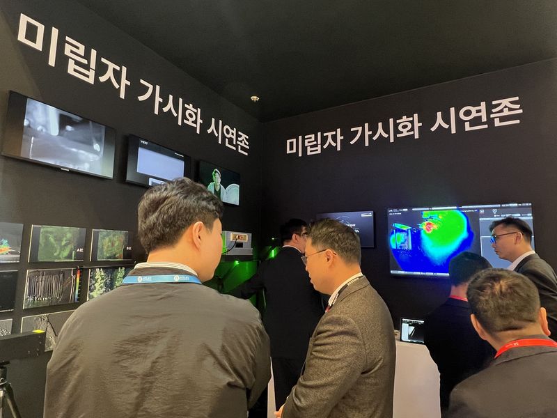
Shinsung E&G set up a particle-visualization demonstration zone in its booth, allowing visitors to experience environmental purification technology used in semiconductor manufacturing processes. The “particle visualization system” on display makes particles generated during semiconductor processes visible to the naked eye.
A Shinsung E&G official said, “As semiconductor processes become more advanced, humidity, cleanliness and contamination control in cleanrooms determine the competitiveness of semiconductor production.” The official added, “Visitors to our booth will be able to see firsthand our technological capabilities across the entire cleanroom environment, from humidity control to identifying sources of contamination.”
Jusung Engineering showcased its “Guidance Series” deposition equipment, which coats semiconductor wafers with metal and nonmetal films. The company prominently featured its atomic layer thin-film growth (ALG) equipment, part of the Guidance Series, which it successfully exported to overseas markets for the first time this year.
Demand for the ALG method, unveiled by Jusung Engineering for the first time in the industry, is likely to increase as semiconductor circuit linewidths continue to shrink. Once linewidths reach 10 nm or below, it becomes difficult for conventional deposition methods to coat the required materials evenly across a wafer. Applying the ALG method, in which the required materials grow on the wafer, can overcome these limitations of deposition technology.
HANMI Semiconductor Co., Ltd. unveiled equipment including a Thermo-Compression Bonder (TC bonder) for high-bandwidth memory (HBM) processes, a 2.5D TC bonder for artificial intelligence (AI) system semiconductor processes, and a flip-chip bonder (FC bonder). The company continues to hold the global No. 1 position in the market for TC bonders used in HBM processes. TC bonders use controlled heat and pressure to precisely bond DRAM memory chips together vertically.
HANMI Semiconductor Co., Ltd. also unveiled its “Micro Saw & Vision Placement system (MSVP),” another pillar of its business alongside TC bonders. The equipment cuts and separates chips on a semiconductor wafer, then washes, dries, inspects, sorts and loads them. HANMI Semiconductor Co., Ltd. remains the global market leader in this equipment as well as in TC bonders.
Shinsung E&G Executive Director Kim Shin-woo, who attended the event, said, “Large crowds are flocking to this year’s Semiconductor Exhibition, reflecting the global supercycle.” He added, “The pace at which semiconductor companies are expanding production capacity is having a major impact on the artificial intelligence (AI) industry. Against that backdrop, it is notable that MPE companies in the semiconductor sector have brought differentiated technologies that can help shorten construction periods and improve semiconductor yields.”
[email protected] Kang Kyung-rae Reporter