Unpacking ‘gum arabic’... An eco-friendly semiconductor that disappears in water [Unboxing Lab]
- Input
- 2026-10-07 05:56:00
- Updated
- 2026-10-07 05:56:00
Remember the excitement of opening a delivery box? Even now, university labs are making remarkable discoveries that could change our lives. They’re simply wrapped in the thick packaging of academic papers. In ‘Unboxing Lab,’ instead of complicated equations and theories, we’ll pick out and package just the things you want to know. So, shall we open the box? Today’s discovery to unbox is this study.
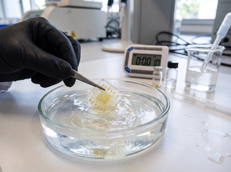
The device developed by the team could be used in electronic products designed to be discarded after a certain period of use. Potential applications include wearable sensors attached to the body to monitor health and disposable electronic devices intended for short-term use.
■ Semiconductors made with a natural substance that dissolves in water
The team focused on gum arabic, which is obtained from acacia trees. Gum arabic is a natural substance that dissolves easily in water.
The team dissolved the substance in water to make the insulating layer of the semiconductor device. The insulating layer controls the amount of electricity flowing through a semiconductor. While organic solvents have sometimes been used to make such layers, the team found a way to make one using water and gum arabic.
The team tested gum arabic concentrations of 20%, 30% and 40% to determine which conditions would produce the best device.
The best results came with a concentration of 30%. The resulting insulating layer had a very smooth surface, measuring about 1.6 nanometers. A nanometer is one-billionth of a meter. The layer was also transparent enough to let through more than 90% of visible light.
Its dielectric constant, which indicates its ability to store electrical charge, was about 27. The dielectric constant of PMMA, used as a comparison, was about 3. The value for the gum-arabic insulating layer was about nine times higher.
A strong ability to store electrical charge makes it possible to accumulate charge inside a semiconductor even at low voltages. This was one reason the team was able to operate the device at a low voltage.
The team deposited an organic semiconductor material called DNTT on top of the insulating layer. The resulting device is a thin-film transistor, in which a pathway for electrical current is formed. Put simply, it is a device that uses small electrical signals to control the flow of electricity.
■ Operates at ±3 V... records an average of 8.90
To assess performance, the researchers measured 16 devices made under the same conditions. Devices made with gum arabic at a concentration of 30% had an average charge-carrier mobility of 8.90 cm2/V·s, while the top-performing device recorded 20.72 cm2/V·s.
Charge-carrier mobility measures how easily electricity moves through a semiconductor. The higher the number, the more easily electricity flows.
The significant reduction in voltage is particularly notable. The gum-arabic device operated stably at ±3 V. By contrast, the PMMA device used for comparison required a voltage of about ±20 V, and its charge-carrier mobility was only about 0.2 cm2/V·s.
In other words, the gum-arabic device operated at a much lower voltage than the comparison device while delivering better electrical transport performance.
The team believes the smooth surface of the gum-arabic insulating layer helped improve performance. The smoother surface allowed the DNTT molecules deposited on it to arrange evenly, reducing obstacles to the flow of electricity. In fact, the gum-arabic device also had fewer defects that hindered electrical flow than the PMMA device.
The device’s stability was also confirmed. Its performance did not decline significantly even when voltage was applied repeatedly. The performance difference observed when the voltage was raised and then lowered again was also small, at about 0.4 V.
The team made and tested devices multiple times to check whether the experimental results were a coincidence. It made 16 devices each using gum arabic at concentrations of 20%, 30% and 40%, as well as 16 PMMA comparison devices, producing them in three separate rounds. The proportion of devices successfully fabricated exceeded 95% under all conditions. The difference in charge-carrier mobility remained within 8% even when the devices were made at different times.
■ Starts dissolving 10 seconds after being placed in water
The team also examined how the device changed when placed in water after use.
When the completed device was submerged, the gum-arabic insulating layer began to turn cloudy and peel away after about 10 seconds. After about 30 seconds, it had dissolved completely. The paper explains that the device retained its shape before being placed in water, but the gum-arabic component dissolved quickly after submersion.
Under normal conditions, however, it did not dissolve easily. The gum-arabic film remained stable in typical environments with humidity below 50%. The team confirmed that it retains its shape during use but rapidly disappears when it comes into contact with water.
This property could be used to make electronic devices intended to be discarded after a set period of use. Potential applications include wearable sensors attached to the body for a limited time to measure information before being removed, as well as disposable electronic devices with short lifespans.
The significance of this study lies in its consideration not only of semiconductor performance but also of the manufacturing process and disposal after use. Gum arabic can be dissolved in water to make the insulating layer, the device can operate at low voltage, and the layer can be removed by placing the device in water after use.
The findings were published in the international materials science journal Advanced Functional Materials. Researchers Im Mirinae, Jang Hyo-won and Swarup Biswas were joint first authors, and Professor Kim Hyuk led the study as corresponding author.
[email protected] Kim Man-gi Reporter