Glass Substrates Move Beyond “Dream Material” Status to Face a Commercial Performance Test... Orders and Yields Will Separate Winners from Losers
- Input
- 2026-09-29 10:39:40
- Updated
- 2026-09-29 10:39:40
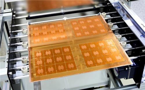
[Financial News] As commercialization of glass substrates, a next-generation semiconductor packaging material, moves forward, securing customers and achieving mass-production yields have emerged as key variables that will determine the competitiveness of related companies. Demand is expected to grow as AI semiconductors become larger, but analysts say reliability validation and cost competitiveness are necessary for that demand to translate into actual sales.
According to the securities industry on the 29th, investment criteria for the glass substrate industry are shifting from technology development and production-facility expansion to concrete business achievements such as customer qualification and orders. As production schedules are delayed and firm demand has yet to become sufficiently clear, evidence demonstrating commercial viability has become increasingly important.
Glass substrates are considered a material capable of overcoming the limitations of conventional organic substrates. As the use of high-bandwidth memory (HBM) in AI semiconductors increases and packages combining multiple chips become larger, problems such as substrate warping and reduced reliability caused by differences in thermal expansion between materials have come to the fore.
Glass offers high planarity and has thermal expansion characteristics close to those of silicon, making it suitable for large-area packaging. However, it is prone to breaking under impact, and microcracks can occur during processing, making it essential to secure stable mass-production technology.
Park Hee-chul, a senior research analyst at Kyobo Securities, said, "A roadmap that only presents a target date is insufficient." He added, "Sharing data on the qualification stages and yield trends is a key task."
In South Korea, Samsung Electro-Mechanics, SK Absolics and LG Innotek are pursuing the commercialization of glass substrates. Samsung Electro-Mechanics is operating a pilot line at its Sejong Plant and conducting evaluations of customer samples. Its target for full-scale mass production is 2028. The company is expanding its product portfolio from conventional semiconductor package substrates to glass substrates while securing key process technologies, including through-glass via (TGV) formation, metal filling and surface processing.
SK Absolics has secured a production facility in Georgia, but customer qualification and demand generation remain challenges. LG Innotek is developing the technology based on a pilot production line and pursuing a strategy of expanding its business in line with market demand.
Globally, attention is focused on whether Intel will adopt the technology commercially. Intel is pursuing a packaging approach that combines silicon bridges inside a glass core to connect chips, thereby simplifying the package structure and improving performance and power efficiency.
Park said, "Intel has a strong incentive to actively pursue the adoption of glass substrates to enhance its foundry competitiveness." However, he pointed out, "As the commercial timeline and customers have not been disclosed, it is necessary to verify whether the expansion of partnerships will actually lead to mass production."
The adoption of TSMC’s panel-based packaging technology, ‘CoPoS,’ should be distinguished from the mass production of glass substrates. Changing the production method from round wafers to square panels and changing the substrate’s core material to glass are separate issues. TSMC’s commercialization of glass-core substrates is forecast to take place after 2030, following the establishment of CoPoS. Initial sources of demand are expected to include network semiconductors and the co-packaged optics (CPO) sector, which packages optical components together with semiconductors. Glass can enable electrical and optical signal paths to be implemented together. Advanced AI accelerators and application-specific integrated circuits (ASICs), which require large-area packaging, have also been cited as potential sources of demand.
Park forecast, "The disclosure of quantitative data on the prerequisites for mass production and whether parity has been achieved is expected to determine the market’s confidence in the commercial viability of the business." He added, "Whether companies can secure costs equivalent to those of existing technologies, and whether customer qualification and orders actually materialize, will determine the revaluation of related companies."
[email protected] Choi Doo-sun Reporter