Multilayer Graphene Directly Deposited at 'Room Temperature'... Next-Generation Composite Conductor Manufacturing Technology Secured
- Input
- 2026-09-27 12:00:00
- Updated
- 2026-09-27 12:00:00
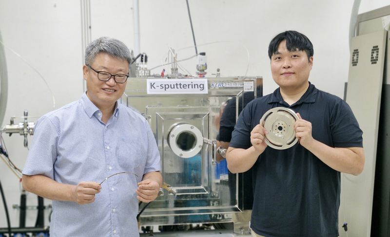
Dr. Kim Ho-seop's team identified the fundamental cause that interferes with graphene formation and independently developed a DC-based K-sputtering system and process that precisely controls the conditions under which carbon particles align on the substrate.
The key was to implement epitaxial growth, in which carbon atoms do not scatter randomly across the surface but instead line up and accumulate along the fine texture of the underlying substrate. This enabled the team to directly grow everything from extremely thin graphene consisting of one or two layers to graphite made up of multiple layers at room temperature, without intense heat. Within the scope of the researchers' survey, this is the world's first achievement in directly producing such an orderly carbon thin film using conventional Sputtering.
To enhance the reliability of the results, the research team collaborated with Professor Kim Jun-ho's team at Incheon National University and Professor Sehee Lee's team at Kyungpook National University (KNU). The researchers used advanced equipment for Raman spectroscopy, atomic force microscopy (AFM), transmission electron microscopy (TEM), and crystallographic orientation analysis (EBSD) held by the respective institutions. They cross-validated the structure and properties of the thin films multiple times, fully demonstrating the technology's objectivity.
The significance of this achievement lies in opening a new path to directly produce high-quality multilayer graphene at room temperature using only Sputtering, an existing thin-film manufacturing technology. In particular, the technology makes it possible to alternately stack materials such as copper and graphene in any desired number of layers within a single system, without a separate and complex transfer process. This is expected to firmly establish the foundation for core manufacturing technology needed for the mass production of next-generation high-performance composite conductors.
KERI researcher Dr. Kim Ho-seop said, "After extensive trial and error, we experimentally confirmed that graphene-based thin films with regularly aligned carbon atoms can be produced using Sputtering," adding, "We will scale up the equipment and develop a continuous production process to commercialize high-performance composite conductors for power equipment, made by alternately stacking copper and graphene, and strengthen Korea's competitiveness in materials, parts, and equipment."
The achievement was recently published in Surface & Coatings Technology (IF 6.9), a top-tier international Q1 journal in the field of materials surface and coating technology. The team has also filed applications for three domestic patents and one foreign patent to protect the technology.
[email protected] Yeon Ji-an Reporter