“We’ll Provide All the Power and Water You Need”: Japanese Competition to Attract Investment Intensifies on SK Speculation [On the Ground]
- Input
- 2026-09-14 06:00:00
- Updated
- 2026-09-14 06:00:00
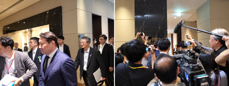
【Financial News Tokyo = Hye-jin Seo, correspondent】After a Korea-Japan symposium on measures to address the declining birthrate ended in Sendai, Miyagi Prefecture, on the 30th of last month, more than a dozen Japanese reporters and several Korean reporters surrounded SK Group Chairman Chey Tae-won. Questions poured in, including, “Are you really planning to invest in Japan?” and “Is it true that you are building a plant in Miyagi Prefecture?” One Japanese reporter blocked Chey’s path and pleaded, “Please, just say one word.” Chey left the venue with his lips tightly sealed.
A Japanese reporter I met at the scene said, “The area was thrown into a frenzy after reports emerged that SK was investing in Miyagi Prefecture.” At the time, neither a site nor plans had been decided for SK hynix to build a plant in Japan.
In an interview with Bloomberg News the following day, Chey said, “We are looking across Japan,” adding that any location with abundant electricity and water would be considered. In an interview with The Asahi Shimbun on the 1st of this month, he described joint production with Japanese semiconductor company KIOXIA as “one option.” The Asahi Shimbun reported that SK had received investment-attraction proposals from several Japanese local governments.
SK stressed that construction of a joint-venture plant in Japan had not been finalized. Although no investment site has been selected, the competition among Japanese local governments to attract the investment is already heating up.
■ Up to 35 billion won for a 30-hectare site: Local governments put conditions on the table
More than 30 hectares remain available at the Second Sendai Northern Core Industrial Park in Ohira Village, Miyagi Prefecture. The site can receive industrial water and ultra-high-voltage electricity, and its location about 24 kilometers from central Sendai is advantageous for securing workers.
Miyagi Prefecture Governor Yoshihiro Murai emphasized at a press conference on the 26th of last month, “It can secure industrial water and electricity, and it is also close to central Sendai,” adding, “Even by global standards, places as good as this are rare.” He also called semiconductors “one of the industries we most want to attract.”
New plants that meet investment and employment requirements receive support equivalent to 10% of the investment, up to 4 billion yen, or approximately 35 billion won. However, Governor Murai said he had received no information regarding the speculation about an SK investment. It has not been confirmed whether the site and incentives were conditions presented specifically to SK.
Other regions are highlighting their own strengths. Chitose City in Hokkaido is improving water infrastructure and roads to support the Rapidus plant. Yokkaichi City in Mie Prefecture is home to a KIOXIA production base, while related companies have gathered in Kyushu around TSMC’s plant in Kumamoto. None of these areas has been officially designated as an SK candidate site, but all have electricity, water, labor, and supply chains.
Behind the competition to attract investment is Kumamoto’s experience in bringing in Taiwan Semiconductor Manufacturing Company (TSMC), the world’s largest foundry. After TSMC began operating its first plant in 2024, investment by suppliers as well as in housing and commercial facilities followed, and tax revenues also increased. Kyushu Financial Group and the Institute for Regional Economy estimated the economic ripple effect from 2022 to 2031, including TSMC’s entry, at approximately 11.2 trillion yen, or about 98 trillion won.
Local governments that have watched these changes are coming to Tokyo to seek out companies. At a corporate-location seminar held by Miyagi Prefecture in August last year, 149 organizations and 254 people attended. Governor Murai and the heads of municipalities in the prefecture personally explained the investment environment.
In January this year, Kumamoto Prefecture Governor Takashi Kimura held a semiconductor corporate-location seminar in Tokyo. He introduced Kumamoto as “a hub for developing new businesses” and called for additional investment.
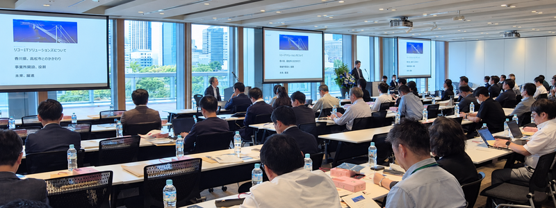
More than 100 people, including company representatives, attended a corporate-location briefing for Kagawa Prefecture that this reporter visited on the 10th. After presentations by Governor Toyohito Ikeda and representatives of NVIDIA and Ricoh IT Solutions, attendees exchanged business cards and continued consultations on potential sites.
Kagawa Prefecture provides large-scale data centers with support equivalent to 10% of their equipment investment and covers 50% of electricity and telecommunications costs. It also expanded the support ceiling for large-scale investments from 500 million yen, or approximately 4.4 billion won, to as much as 5 billion yen, or approximately 43.8 billion won. The day after the briefing, Kagawa was selected as the only area in Chugoku and Shikoku designated by the Japanese government as a “GX Strategic Region for Data Center Clusters.”
■ Beyond plants to R&D and AI hubs
Japan’s targets for investment attraction are not limited to production plants. On the 8th, Samsung Electronics opened the Advanced Packaging Laboratory (APL), an advanced semiconductor packaging research hub in Yokohama, at a cost of 40 billion yen, or approximately 350 billion won. The Japanese government provided 22.5 billion yen, or more than half of the investment, equivalent to approximately 196.9 billion won. The facility, which covers about 6,600 square meters, includes a cleanroom and analytical equipment comparable to those used on an actual production line. Ninety-five Korean and Japanese researchers work there.
APL is closer to a mass-production site than a conventional research institute. Samsung Electronics is evaluating back-end materials for AI semiconductors, including high-bandwidth memory (HBM) and three-dimensional integrated circuits, with about 50 Japanese materials and equipment companies, and is even producing prototypes. It can cut by up to two months the time previously required to send materials made in Japan to Korean plants for testing. In effect, Japanese materials, parts, and equipment companies have been directly connected to Samsung Electronics’ development and verification process.
SK’s Japanese production facilities remain under consideration, but Samsung has already begun R&D in Japan integrated with the local supply chain. Japan’s competition to attract companies is also expanding beyond simply offering plant sites and subsidies to bringing in R&D, advanced packaging, and AI and data-center ecosystems.
In Sendai, reporters waited for Chey’s answer, while in Tokyo governors offered companies sites, electricity, water, and subsidies. Kumamoto’s experience—where a single hub transformed regional employment, tax revenues, and industrial structure—is driving Japanese local governments to act.
[email protected] Hye-jin Seo Reporter