Hanyang University Undergraduate Solves Challenge of ‘Power-Hungry’ AI Semiconductors
- Input
- 2026-09-09 21:33:35
- Updated
- 2026-09-09 21:33:35
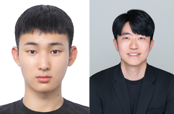
[Financial News] An undergraduate student at a Korean university has developed next-generation technology that can dramatically reduce the power consumption of artificial intelligence (AI) semiconductors while significantly shrinking chip size. The technology simultaneously handles AI computation and data storage within a single component, offering a potential breakthrough for addressing power shortages at AI data centers and limits on component integration.
Hanyang University announced on the 9th that a research team led by Lee Da-hoon, a fourth-year student in the Department of Materials Science and Engineering and the paper’s first author, and Professor Kim Hyung-jin, the corresponding author, developed a core technology for next-generation ultra-low-power AI semiconductors. The team’s paper was published in the internationally renowned journal Nano Energy.
The key achievement is that the team overcame the limitations of In-Memory Computing with just one component, or device.
Conventional computers separate the “warehouse,” or memory, where data is stored from the “workshop,” or processor, where calculations are performed. When handling massive computations such as those required by AI, data constantly moves between the two, consuming enormous amounts of power and creating a bottleneck that slows processing. In-memory semiconductors, which perform calculations directly within the memory itself, have attracted attention as a solution. However, until now, multiple memory components had to be interconnected to perform a single calculation, limiting efforts to reduce chip size.
Breaking with conventional thinking, the research team completed “1C-XNOR,” a technology that simultaneously performs core AI calculations and stores data within a single memory cell, or device. It compresses the complex process by which AI rapidly classifies vast amounts of data as zeros and ones into a single device.
The technology was designed to be compatible with the NAND flash memory structure widely used today, making it easier to apply to actual semiconductor manufacturing processes in the future. It can enable denser component integration while dramatically reducing power consumption, giving it broad potential applications ranging from small mobile devices to large-scale data centers.
The research drew attention from academia and industry because it was led throughout—from semiconductor device fabrication to verification of AI computations—not by master’s or doctoral students, but by a fourth-year undergraduate researcher.
Lee Da-hoon said, "It was meaningful to lead research that involved fabricating semiconductor devices myself as an undergraduate and connecting them to actual AI computations." He added, "I will continue researching ways to connect memory and AI semiconductors."
Professor Kim Hyung-jin, who supervised the research, emphasized, "We demonstrated the feasibility of highly integrated, ultra-low-power AI semiconductors by reducing the number of components previously required from several to just one." He added, "This is a highly meaningful example of an undergraduate student taking the lead in research and achieving results as the first author in a world-renowned academic journal."
The research was conducted through the Ministry of Science and ICT and the National Research Foundation of Korea (NRF)’s Innovation Research Center Program, Next-generation Intelligence-Type Semiconductor Development Program, and Young Researcher Support Program. The findings were first published online by Nano Energy and are scheduled to appear in the journal’s official November issue.
[email protected] Man-ki Kim Reporter