YMT to Unveil Large-Area TGV Samples at KPCA Show 2026, Targeting Next-Generation Semiconductor Materials Market
- Input
- 2026-09-09 17:43:35
- Updated
- 2026-09-09 17:43:35
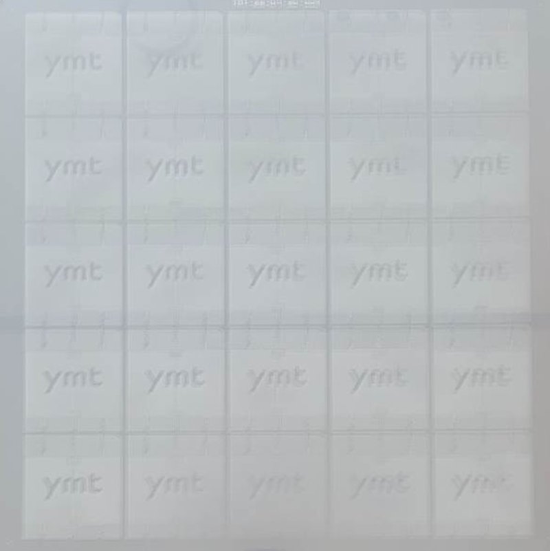
[Financial News] YMT, a company specializing in electronic materials, is targeting the next-generation semiconductor packaging market with full-size Through Glass Via (TGV) glass substrates and its new Electroless Nickel Electroless Palladium Immersion Gold (ENEPIG) products.
YMT announced that it will participate in KPCA Show 2026, held from the 9th to the 11th at Songdo Convensia in Incheon, where it will showcase TGV technology for next-generation semiconductor packaging and new ENEPIG products.
The centerpiece of this exhibition is TGV glass substrates for next-generation semiconductor packaging. YMT will unveil two actual TGV glass-substrate samples produced at the 510×515mm full-size scale. The samples demonstrate the implementation of a TGV plating process on actual large-area glass substrates, going beyond small test coupons.
TGV is a technology that forms fine vias in a glass substrate and fills them with metal to create electrical pathways. It is attracting attention as a next-generation semiconductor packaging substrate technology. The key technical challenge is to secure adhesion between the glass and plating layer while suppressing cracks that may occur during processing due to the properties of glass. As substrates become larger, process technology capable of ensuring uniform plating quality and adhesion across the entire surface becomes increasingly important.
At the exhibition, YMT will present both a method that uses a separate sputtering process and a Sputter-Free method that omits sputtering. The company plans to demonstrate its ability to support both approaches according to customers’ process conditions and required specifications. It developed the processes with a focus on improving cracking issues in glass substrates under both methods by applying new pretreatment technology.
The TGV business is expanding beyond research and development into the customer evaluation stage. YMT is currently supplying TGV samples with plating completed to numerous companies in Korea and abroad, and continues to provide evaluation samples to global big tech companies.
YMT is also building infrastructure for mass production. Its affiliate YPT has proactively ordered equipment for TGV mass production and is targeting setup in the fourth quarter of this year. YMT said, "In line with customer evaluations and future market expansion, we plan to advance TGV process technology while building mass-production infrastructure."
YMT will also introduce new products and expand their applications based on its accumulated technological expertise and mass-production competitiveness in the ENEPIG field. ENEPIG is a surface-treatment process that sequentially forms nickel (Ni), palladium (Pd), and gold (Au), and is used in semiconductor packaging and high-performance electronic substrates that require high bonding reliability.
YMT has secured competitiveness in the ENEPIG market through its long-standing surface-treatment technology and experience in mass-production supply. In particular, it has demonstrated its technological and quality competitiveness through global customers, including mass-producing and supplying ENEPIG products for network boards made by a North American graphics-chip company.
At this exhibition, YMT will further broaden its product portfolio based on the competitiveness of its existing ENEPIG business. It will newly unveil KCN-Free ENEPIG, which reduces the use of hazardous substances, and is currently conducting application tests with numerous customers.
YMT will also exhibit ENEPIG products for optical modules in response to rising demand for optical modules driven by the expansion of the artificial intelligence (AI) data center and high-speed network markets. The strategy is to extend its surface-treatment technology and mass-production expertise, accumulated in the semiconductor and network-board sectors, to optical modules and meet demand from next-generation data centers and high-speed communications markets.
A YMT official said, "At KPCA Show 2026, we plan to directly demonstrate our technological development achievements and ability to respond to customer-specific processes through an actual 510×515mm large-area TGV sample. We will proactively prepare for the transition of the TGV business to mass production by conducting global customer evaluations and building mass-production infrastructure in parallel. In ENEPIG, we will continue expanding application areas to include KCN-Free and optical-module products, based on our proven technological expertise and mass-production competitiveness."
An industry official said, "The competitiveness of next-generation semiconductor packaging materials depends not only on technological implementation but also on securing reproducible quality tailored to customers’ process conditions and the ability to provide stable mass-production supplies. The parallel progress of customer evaluations for large-area TGV samples and mass-production infrastructure development will be a key indicator of the industry’s readiness for commercialization."
[email protected] Choi Doo-sun Reporter