Samsung Electro-Mechanics to Participate in 'KPCA Show 2026,' Showcase Next-Generation Semiconductor Package Substrate Technologies
- Input
- 2026-09-09 11:51:40
- Updated
- 2026-09-09 11:51:40
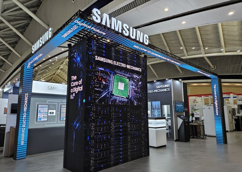
[Financial News] Samsung Electro-Mechanics is strengthening its competitiveness in next-generation package substrates featuring large-area and high-layer-count technologies in response to the expanding artificial intelligence (AI) semiconductor market.
Samsung Electro-Mechanics announced on the 9th that it will participate in KPCA Show 2026, the International Semiconductor Substrate and Advanced Packaging Industry Exhibition, held at Songdo Convensia in Incheon through the 11th, where it will showcase next-generation semiconductor package substrate technologies.
KPCA Show is a leading exhibition in Korea where domestic and international companies specializing in semiconductor substrates and packaging, materials, and equipment participate to share the latest technologies and market trends in the related industries. Semiconductor package substrates are key components that connect highly integrated semiconductor chips with mainboards and transmit electrical signals and power.
As the performance of semiconductors such as AI accelerators and server CPUs rapidly improves and the use of high-performance memory expands, package substrates are evolving beyond simple connectivity to become a core technology that determines semiconductor performance, power efficiency, and signal stability. AI semiconductors, in particular, require advanced technologies, including large-area and high-layer-count substrates, fine circuits, fine vias and bumps, and high-precision embedding.
At this exhibition, Samsung Electro-Mechanics will introduce next-generation package substrate technologies covering a range of applications, from AI and servers to data centers, mobile devices, and autonomous driving. The products include 2.5D package substrates, 2.1D package substrates, glass substrates, automotive FC-BGA, and UTCSP substrates.
As generative AI spreads and the computing performance of AI accelerators rises, data input and output (I/O) is increasing sharply. Accordingly, substrates must support large-area, high-layer-count structures, high circuit density, and the implementation of large numbers of bumps.
Samsung Electro-Mechanics will present core technologies for 2.5D package substrates for AI accelerators, including technologies that reduce warpage in large-area, high-layer-count substrates, high-speed signal transmission, and high-density interconnection. It will also showcase 2.1D package substrate technology, which enables direct connections between semiconductor chips without a silicon interposer.
As AI semiconductors become larger and more highly integrated, the need is growing for substrate technologies that offer greater rigidity and dimensional stability than conventional organic-material-based substrates and can improve signal, power, and heat-dissipation characteristics.
Glass substrates use glass as the core material to reduce substrate warpage and secure signal performance and power efficiency while lowering the number of layers. At the exhibition, Samsung Electro-Mechanics will introduce key glass-substrate technologies, including forming fine interconnection channels in glass materials and filling them with metal, as well as precision surface-processing technology.
In addition, Samsung Electro-Mechanics' UTCSP substrate addresses the demand for high integration and slimmer designs in data centers and mobile devices through a coreless structure that reduces substrate thickness and fine bond-finger technology. The company will also display UTC package substrates used in CPUs for laptops and tablets, along with co-package substrates for smartphones. Automotive package substrates require reliability that can withstand high temperatures, high humidity, and repeated temperature changes, in addition to large-area and high-layer-count structures and fine-circuit implementation. Samsung Electro-Mechanics is strengthening its competitiveness in package substrates for autonomous driving through high-functionality substrate technologies, including multi-chip structures, and reliability-enhancement technologies.
Joo Hyuk, executive vice president of Samsung Electro-Mechanics and head of the Package Solution Business Unit, said, "As high-performance semiconductor markets such as AI accelerators, servers, and autonomous driving continue to grow, the role and technological complexity of package substrates are rising rapidly. Samsung Electro-Mechanics will advance large-area, high-layer-count, ultra-fine-circuit, and next-generation packaging technologies to compete in the high-end semiconductor package substrate market."
[email protected] Joo Hyuk Reporter