Samsung’s Counterattack After Falling Behind in HBM: Technology Alliance with 50 Japanese Companies
- Input
- 2026-09-08 17:44:32
- Updated
- 2026-09-08 17:44:32
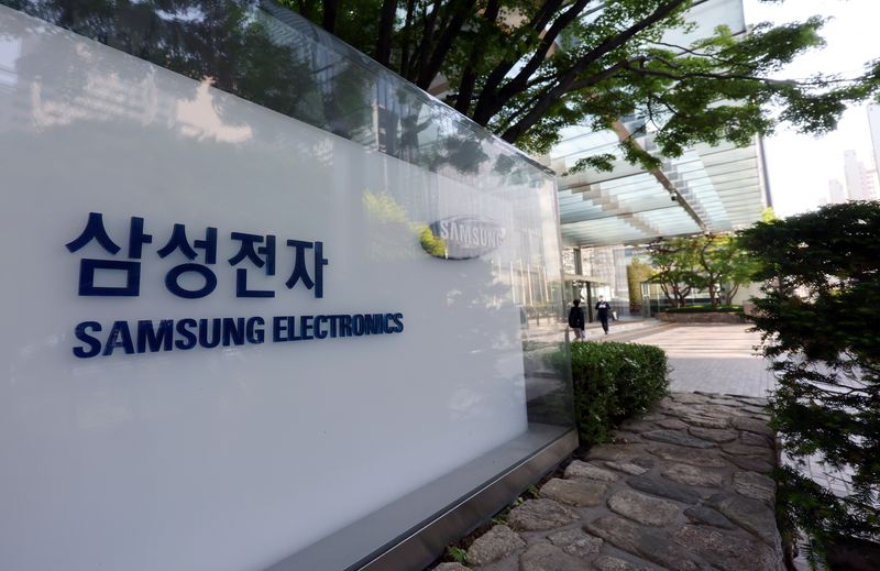
【Financial News, Tokyo—Correspondent Hye-jin Seo】Samsung Electronics has joined forces with more than 50 Japanese semiconductor materials and equipment companies to strengthen its competitiveness in artificial intelligence (AI) semiconductors. Its strategy is to leverage Japan’s advanced packaging technology to catch up with SK hynix in the high-bandwidth memory (HBM) market.
According to Japanese media outlets, including The Nikkei, on the 8th, Samsung Electronics held an opening ceremony for its advanced semiconductor back-end process research center, Advanced Package Lab (APL), in Minato Mirai, Yokohama, that day. The company invested a total of 40 billion yen, while the Ministry of Economy, Trade and Industry of Japan (METI) is providing 22.5 billion yen in support.
Samsung Electronics Vice Chairman Jun Young-hyun, who also heads the Device Solutions Division, said, "We will accelerate Korea-Japan technology exchanges and turn them into a driving force for the joint growth of the next-generation packaging industry."
APL covers approximately 6,600 square meters and is equipped with cleanrooms similar to those used on actual production lines. Ninety-five Korean and Japanese researchers will evaluate back-end process materials and develop mass-production technologies. Fifteen major Japanese suppliers, including Tokyo Electron and Ibiden, attended the opening ceremony.
As semiconductor miniaturization approaches its limits, the focus of performance competition is shifting toward advanced packaging, which connects multiple chips such as HBM and graphics processing units (GPUs). A Samsung Electronics official said, "We rely almost entirely on Japanese companies for key HBM materials."
Japan has world-class competitiveness in key back-end process materials for HBM, including adhesives, substrates and encapsulants. Sumitomo Bakelite accounts for about 40% of the global encapsulant market, while Resonac and Mitsubishi Gas Chemical are leading suppliers of substrate materials.
Until now, evaluating materials developed in Japan after bringing them to South Korea took up to two months because of chemical-substance approvals and import and export procedures. Going forward, materials evaluation and prototype production can be completed in Japan, with only validated technologies applied to Samsung’s mass-production lines in South Korea.
Samsung Electronics is the world’s No. 1 memory semiconductor company, but it trails SK hynix in HBM for AI semiconductors. As back-end processing has emerged as a new bottleneck, Samsung is seeking to catch up by leveraging Japan’s materials and equipment technologies.
Improved Korea-Japan relations also supported the investment. Samsung Electronics began considering the establishment of the research center in 2021, when relations between the two countries had cooled, and officially announced its investment plan in December 2023, after shuttle diplomacy between the leaders resumed.
As competition in AI semiconductors expands from a contest among individual companies to one among cross-border industry alliances, attention is focused on the performance of a "Korea-Japan semiconductor alliance" combining Japan’s materials and equipment technologies with South Korea’s mass-production capabilities.
[email protected] Hye-jin Seo Reporter