Samsung Electronics Applies ASML’s Next-Generation Lithography Equipment to Advanced DRAM Manufacturing
- Input
- 2026-09-08 16:29:57
- Updated
- 2026-09-08 16:29:57
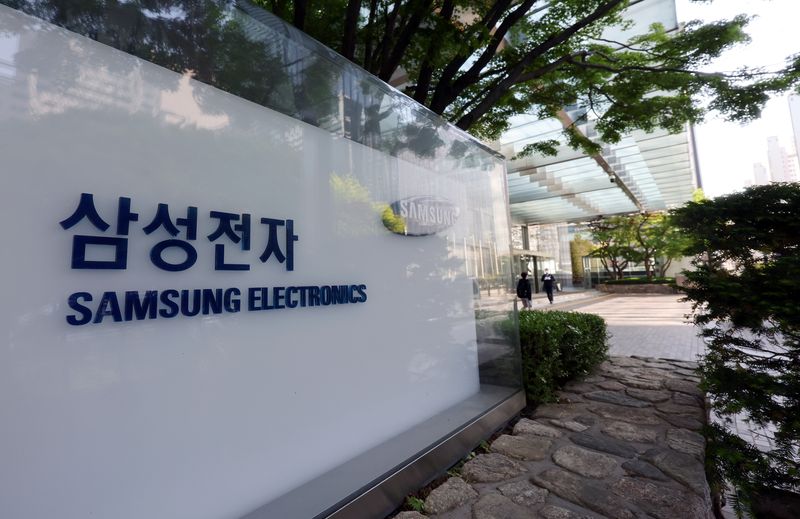
[Financial News] Samsung Electronics is collaborating with Dutch semiconductor equipment maker ASML to introduce next-generation lithography equipment, a key component of advanced DRAM manufacturing processes.
By 2028, Samsung Electronics plans to become the first in the industry to apply next-generation lithography equipment—High-NA EUV equipment—to advanced DRAM manufacturing. The company aims to widen its lead over competitors by enabling further memory scaling and improving productivity. Industry observers say that closer cooperation with ASML, the exclusive supplier of advanced EUV lithography equipment, could mark a major turning point in Samsung Electronics’ efforts to restore its next-generation DRAM competitiveness and secure leadership in the global memory market.
Samsung Electronics said on the 8th that it would participate in the ASML-led large-mask consortium to jointly develop next-generation 12-inch photomasks. It also announced plans to strengthen cooperation with ASML to introduce High-NA EUV into advanced DRAM manufacturing by 2028.
A photomask is a precision mask, or template, engraved with intricate circuit patterns. It is an essential tool used to transfer the patterns designed on a wafer using light. Because the precision of circuit patterning determines semiconductor performance and yield, photomasks are considered a core element of semiconductor manufacturing technology.
The large-mask consortium is a consultative body established to transition from the 6-inch masks used in semiconductor lithography equipment to 12-inch masks. Semiconductor lithography processes have traditionally used 6-inch masks. However, switching to 12-inch masks with the introduction of High-NA EUV would allow more circuits to be patterned on a wafer at once, increasing productivity and lowering chip manufacturing costs.
Samsung Electronics, a leading company in both memory and foundry manufacturing, is expected to play a key role in the consortium’s transition to 12-inch photomasks.
Samsung Electronics also plans to strengthen cooperation with ASML to introduce High-NA EUV into advanced DRAM manufacturing by 2028.
The cooperation between Samsung Electronics and ASML indicates that High-NA technology is ready to be applied to advanced memory manufacturing as well. Through more precise patterning, Samsung Electronics is expected to achieve both further DRAM scaling and improved productivity.
Jun Young-hyun, vice chairman and CEO of Samsung Electronics, said, "Samsung Electronics will continue its leadership in advanced semiconductor manufacturing, including foundry and memory, through innovative technologies and strong partnerships." Christophe Fouquet, CEO of ASML, emphasized, "As we enter a new era driven by AI, we look forward to leading innovation for next-generation semiconductor manufacturing together with Samsung Electronics."
[email protected] Kim Hak-jae Reporter