Samsung Strengthens Strategic Weapon, Lithography Equipment, to Widen Gap with China
- Input
- 2026-09-08 16:52:45
- Updated
- 2026-09-08 16:52:45
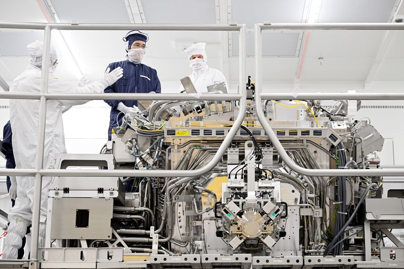
Samsung’s semiconductor division began adopting 1c DRAM, a 10-nanometer-class, sixth-generation process, ahead of its rivals after setting a target of exceeding the standards of the Joint Electron Device Engineering Council from the initial stage of HBM4 development. The next-generation lithography equipment is also reportedly set to be applied to the most advanced process.
Jonghwan Lee, a professor in the Department of Semiconductor Engineering at Sangmyung University, said, "The better the DRAM performance, the better HBM performance inevitably becomes." He assessed, "This cooperation means that Samsung and ASML will jointly develop lithography equipment to further shrink the 10-nanometer process and enable ultra-fine patterning. It has major technological significance."
EUV lithography equipment uses extreme ultraviolet light to etch semiconductor circuits onto wafers and can draw lines as narrow as 13.5 nm in a single exposure. With multipatterning, circuits as small as 2 nm can be produced. The key advantage of the next-generation lithography equipment is that it can reduce the number of multipatterning steps. Existing EUV requires four multipatterning steps to implement 2-nm circuits, while High-NA EUV can theoretically cut the number of process steps in half. The next-generation lithography equipment costs about 500 billion won, but the calculation is that costs could fall substantially if mass production succeeds by halving the number of process steps.
Samsung Electronics plans to be the first in the world to apply next-generation lithography equipment to a mass-produced DRAM product. It will verify the manufacturing process conditions, yield, and productivity at an early stage to determine whether the equipment can contribute to actual large-scale DRAM production.■ Widening the technology gap with China to block its pursuitAnalysts say that by strengthening this strategic weapon, Samsung Electronics will widen its technology gap not only with memory-market rivals SK hynix and Micron Technology, but also with China, which is mounting an aggressive challenge.
The United States struck a critical blow to China’s semiconductor ambitions in 2019, during Donald Trump’s first administration, by banning ASML’s exports of EUV equipment to China. China, however, moved quickly to catch up in the mainstream DRAM market by using deep-ultraviolet (DUV) equipment for multipatterning. According to a Counterpoint Research survey, ChangXin Memory Technologies (CXMT) held a 10% share of the global DRAM market in the second quarter of this year, more than doubling from 4% during the same period last year.
CXMT recently began limited production of fifth-generation HBM3E. Unable to import EUV equipment because of U.S. export controls, the Chinese government is making every effort to develop its own technology for semiconductor self-sufficiency, even deploying state capital. Some observers predict that China will not catch up with ASML’s technological capabilities within the next 10 years, but experts say the gap must be widened because Chinese companies’ technological capabilities are improving rapidly.
Jonghwan Lee said, "China will use every available method to narrow the technology gap, whether by developing lithography equipment domestically or importing it through a third country." He added, "The most important thing for widening the technology gap with Chinese companies again and securing technological superiority over competitors is next-generation lithography equipment."
[email protected] So-hyun Park Reporter