Samsung-ASML Technology Alliance Enters Its 16th Year, Joining Forces on 12-Inch Photomask Transition
- Input
- 2026-09-08 16:33:04
- Updated
- 2026-09-08 16:33:04
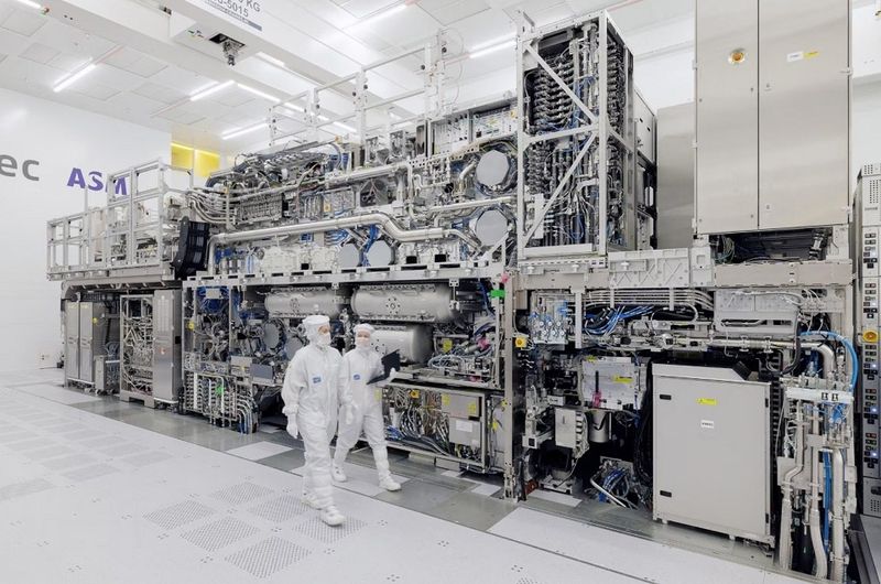
Samsung Electronics’ participation on the 8th in the large-mask consortium led by ASML is aimed at taking the lead in building a 12-inch photomask ecosystem that can fully utilize the capabilities of High-NA EUV.
A photomask is a template containing the original circuit pattern to be printed on a wafer. If the existing 6-inch photomask is used with High-NA EUV, the area that can be patterned at one time is cut in half, increasing the burden on the process. The plan is therefore to expand photomasks to 12 inches, reducing production time and cost pressures.
The cooperation between Samsung Electronics and ASML has evolved beyond a simple equipment supplier-customer relationship into a technology alliance that jointly verifies and commercializes next-generation lithography technologies.
The partnership between the two companies dates back to 2010. At the time, ASML shipped its first pre-production EUV system to Samsung Electronics’ research facility. Even before EUV was broadly applied to advanced semiconductor mass production, Samsung Electronics used ASML equipment to accumulate process experience and verify its mass-production potential.
In 2012, the companies further strengthened their partnership through an equity investment. Samsung Electronics invested €276 million in ASML’s research and development of next-generation lithography technologies and separately acquired a 3% stake. In other words, Samsung Electronics, as a customer, also shared the funding and development burden required for equipment development.
This cooperation led to actual mass production. Samsung Electronics completed development of a 7-nanometer process using EUV in 2018, then shipped the industry’s first system-on-chip (SoC) using a 7-nanometer process in 2019. In 2020, it became the first company in the memory industry to apply EUV to DRAM and establish a mass-production system.
Samsung Electronics later sold its entire stake in ASML, but the two companies’ technological cooperation expanded further. In 2023, they agreed to establish a next-generation semiconductor research fab in South Korea, broadening their partnership beyond equipment supply into research and development.
Samsung Electronics and ASML are now seen as having expanded their cooperation from individual equipment and process development to the establishment of an industrial ecosystem, including the creation of next-generation photomask specifications.
An industry official said, "Samsung Electronics has experience leading the transition from 8-inch to 12-inch wafers in the early 2000s and successfully establishing the new specification in mass-production systems. Since it has experience transitioning manufacturing standards that require multiple equipment and materials companies to move together, Samsung Electronics is expected to play a key role in this transition as well."
[email protected] Ji-yeon Park Reporter