"The semiconductor cycle is now in the bottom of the third inning... Regulations must be eased for proper support" [fn Insight]
- Input
- 2026-08-31 15:51:03
- Updated
- 2026-08-31 15:51:03
It takes about 135 days, or four to five months, to make a single thumbnail-sized high-bandwidth memory (HBM) chip. A wafer is loaded, and then you have to wait four and a half months before one chip comes out. Meanwhile, demand for Artificial Intelligence (AI) keeps rising by the minute. Industry insiders say that only a little more than half of the memory semiconductors required by AI this year will actually be supplied. That is why big tech companies keep pressing Samsung Electronics and SK hynix to deliver chips faster.The AI semiconductor mega-cluster plan, one of the government’s three major mega projects, is a declaration that it intends to close that gap. The government itself has described the effort as a blitzkrieg, underscoring the need for speed. But under the existing process — site selection, environmental impact assessment, land acquisition, and water and power infrastructure — it takes 10 years to build a single factory. Critics say that is far too slow compared with Taiwan Semiconductor Manufacturing Company Limited (TSMC), which built a plant in Kumamoto, Japan, in just 1 year and 10 months.
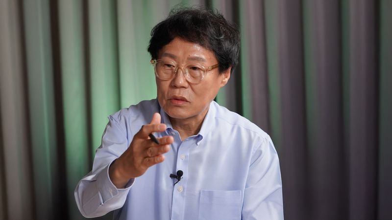
[Financial News] Park Jea-Gun, distinguished professor in the Department of Convergence Electronics Engineering at Hanyang University, said in a meeting with Nodong-il, chief editorial writer at Financial News, on the 31st, "Semiconductors are not a business of scale, but a business of timing." He added, "A system in which the government simply responds to companies’ requests and then builds infrastructure is always too late. We need to completely shift to a 'first infrastructure' paradigm, where infrastructure is built in advance and companies enter according to market conditions." Having joined Samsung Electronics' Giheung plant in 1985 and spent 40 years in semiconductors, he described the current AI cycle as "the bottom of the third inning, or the top of the fourth inning" in baseball terms.
The interview can be viewed on Financial News' YouTube channel, fn Insight.— There are concerns that semiconductors are a cyclical industry, so excessive expansion could backfire.▲ Historically, semiconductors have gone through ups and downs every three to five years. But the average trend has always been upward, and this AI cycle is much longer than usual. I believe the memory shortage will continue at least until 2030. In the past, downturns came because markets such as the internet and smartphones grew and then became saturated. Smartphones were already approaching saturation before COVID-19. But AI keeps creating new markets. I would even say a downturn may not come at all.— If you compare it to a nine-inning baseball game, what inning are we in now?▲ Around the bottom of the third inning or the top of the fourth. So far, growth has been driven mainly by learning, and inference is only now starting to expand rapidly. On top of that come AI agents and on-device AI. By 2030, physical AI will arrive. Once robots and autonomous vehicles are fully deployed, every robot and car will need an AI accelerator, and inside that, the memory we specialize in will also be needed. By 2040, we will be in the era of artificial general intelligence (AGI), as AI experts call it. If new markets keep opening, the game will never really end.— Is the move by big tech companies to make their own chips with neural processing units (NPU) or application-specific integrated circuits (ASIC) a threat to us?▲ On the contrary, it is an opportunity. Google developed Tensor Processing Units (TPU) to move away from NVIDIA Corporation’s ecosystem, but HBM is used there too. Whether it is a GPU, TPU, or ASIC, nothing works without memory. In fact, as each customer’s needs become more specialized, memory becomes more diverse. That is why products such as Compute Express Link (CXL), which aims to maximize memory utilization, and High Bandwidth Flash (HBF), which stacks NAND flash vertically to improve both capacity and speed, are emerging. In the past, the structure was one in which the CPU or application processor pulled memory along behind it. Now, the era is shifting to one in which memory leads the way.— There are also concerns about the rapid catch-up by ChangXin Memory Technologies (CXMT) in China.▲ To be clear, the technology gap is at least three years, and in HBM it is even wider. If anything, the gap appears to be growing. CXMT’s wafer input volume is around 300,000 wafers per month, which is not small, but most of its products are legacy, general-purpose chips. We do not have the capacity to make all of those general-purpose products. It is actually better for them to handle the commodity side while we focus on high-performance, high-value-added products. That said, to maintain the gap, 3D DRAM is the key. The two-dimensional structure has reached its physical limit, so it must be built upward like an apartment building, and it needs to be applied starting in 2029. If CXMT succeeds in mass production first, the entire memory market could be reshaped. Investment in research and development for 3D DRAM must never be delayed, just as much as investment in capacity.— Do you think the special law for the mega-cluster promoted by the government will be effective?▲ I think it will have a very large effect. In Korea, when we plan a semiconductor complex, we conduct environmental assessments, designate the site as a complex, and acquire the land. Land acquisition alone takes four to five years. It is difficult because we are asking people who are living well to move out, and there are also issues with land speculation and blocking tactics. Only after that do we build infrastructure such as water and power. Because everything is done sequentially, it takes 10 years. In Kumamoto, they prepared the site while conducting the environmental assessment and laid the infrastructure at the same time, finishing in 1 year and 10 months. The core of the special law is to carry out all procedures in parallel and in a one-stop manner.— In the end, the biggest obstacles are water and power.▲ That is right. Yongin needs to draw water from the Han River basin, and power must come from Dangjin, the southwest region, and the East Coast of Korea. Since the route passes near the Seoul metropolitan area, underground cabling is necessary, and issues of local acceptance arise. Fab sites in the southwest region are relatively better. There are plans to raise dam levels in the Yeongsan River basin to secure 600,000 tons of water, and power can come from nearby nuclear plants or, if needed, from liquefied natural gas (LNG) plants built alongside them. Solar power is not suitable for semiconductors. Even a one-second outage can cause enormous losses, so stable, high-quality power is essential. The government’s plan is to bring forward four SK hynix fabs to 2032 and six Samsung Electronics fabs to 2040, but in the end, securing infrastructure is the key.
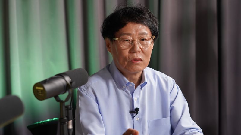
■ Profile of Professor Park Jea-Gun △ Head of the Semiconductor and Materials Technology Group at Samsung Electronics △ Ph.D. in Materials Engineering, North Carolina State University, USA △ Policy adviser in the economic innovation field for Busan Metropolitan City Government △ President of The Korean Society of Semiconductor & Display Technology

[email protected] Han Young-joon Reporter