Samsung 'Computation' vs. SK '20-Layer Stacking'... Next-Generation HBM Battleground is 'Design and Packaging'
- Input
- 2026-08-24 18:26:56
- Updated
- 2026-08-24 18:26:56
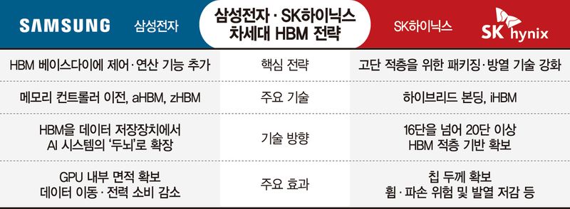
Samsung Electronics unveiled a roadmap to evolve the HBM base die into a "brain" capable of handling even artificial intelligence (AI) computations. SK Hynix officially announced the mass production of its 12-layer HBM4 product, which is to be installed in NVIDIA's next-generation AI accelerator "Vera Rubin," and the entry of its 16-layer product into customer certification. Additionally, it showcased next-generation packaging technology for ultra-high stacking of 20 layers or more.
As competition in AI accelerator performance intensifies, it is assessed that the HBM competition is expanding beyond simple speed and capacity expansion to encompass base dies, ultra-high stacking, and packaging technologies. ■ Samsung Evolves HBM 'Brain' Base Die According to industry sources on the 24th, Samsung Electronics and SK Hynix presented their visions for next-generation HBM side by side at "Hot Chips 2026," held at Stanford University in the United States on the 23rd (local time). Hot Chips, which began in 1989 and is held annually in Silicon Valley, USA, is a leading conference in the fields of high-performance semiconductors and computing architecture.
It serves as a venue where global companies such as NVIDIA, AMD, Intel, and IBM unveil cutting-edge technologies to be applied to actual products, including next-generation CPUs, GPUs, AI accelerators, memory, and packaging. By focusing on actual products and implementable technologies rather than academic research, it is considered a platform to glimpse the future direction of semiconductor technology evolution. At this year's Hot Chips, Samsung Electronics and SK Hynix agreed that GPUs, HBM, foundry, and packaging must be designed as a single system to resolve the bottlenecks in AI semiconductors, yet they presented different solutions.
Samsung Electronics focused on advancing the base die of its HBM. The base die is a semiconductor located at the very bottom of the HBM that controls the transmission of data, power, and signals between the DRAM and the GPU. Samsung Electronics proposed a plan to move some GPU functions, such as the memory controller, to the base die and utilize the freed-up space for computational cores.
The explanation is that relocating the memory controller, which occupies about 5–10% of the GPU area, can lead to a 10–20% performance improvement. They also presented 'aHBM,' which reduces data transfer and power consumption by directly processing some AI computations on the base die. An industry insider stated, "Samsung Electronics has focused on evolving the base die from a simple data conduit into a 'brain' responsible for some functions of the AI system," adding, "This is an approach that leverages Samsung Electronics' strengths in possessing capabilities in memory, foundry, and packaging.
" In the long term, the plan is to advance to 'zHBM,' which vertically combines the GPU and DRAM. Currently, the GPU and HBM are connected side-by-side, but this involves directly connecting the two chips vertically to reduce data transfer distances. 3 times compared to HBM4E.
■ SK Goes Beyond 12 & 16 Layers to 20-Layer HBM Battle SK Hynix has focused on advanced packaging technology to resolve issues regarding heat generation, thickness, and reliability that arise during the process of stacking HBM layers higher. In particular, the company officially announced today that its HBM4 12-layer product is currently in 'production,' and that the 16-layer product has entered the 'qualification' stage. This reaffirms that the mass production of the HBM4 12-layer is proceeding normally, while also concretizing that the development of the 16-layer product has progressed to the customer certification stage.
The company also presented 'hybrid bonding' technology for future HBM layers of 20 or more. This method eliminates existing bumps and fillers to directly connect chips, thereby reducing the gap between chips and increasing the number of layers without making the DRAM excessively thin. They also unveiled 'iHBM' to reduce heat generation.
This technology lowers thermal resistance by more than 30% compared to existing standards by creating a separate heat dissipation channel. An industry insider commented, "While the focus of competition in the past was on the performance of the DRAM itself, the center of gravity of the competition for next-generation HBM is shifting to the base die and packaging.
"
[email protected] Garden day Reporter