TSMC Races Ahead in AI Chip Packaging... Samsung Electronics Puts Full Effort into HBM, Foundry, and Packaging Capabilities
- Input
- 2026-08-14 06:59:00
- Updated
- 2026-08-14 06:59:00
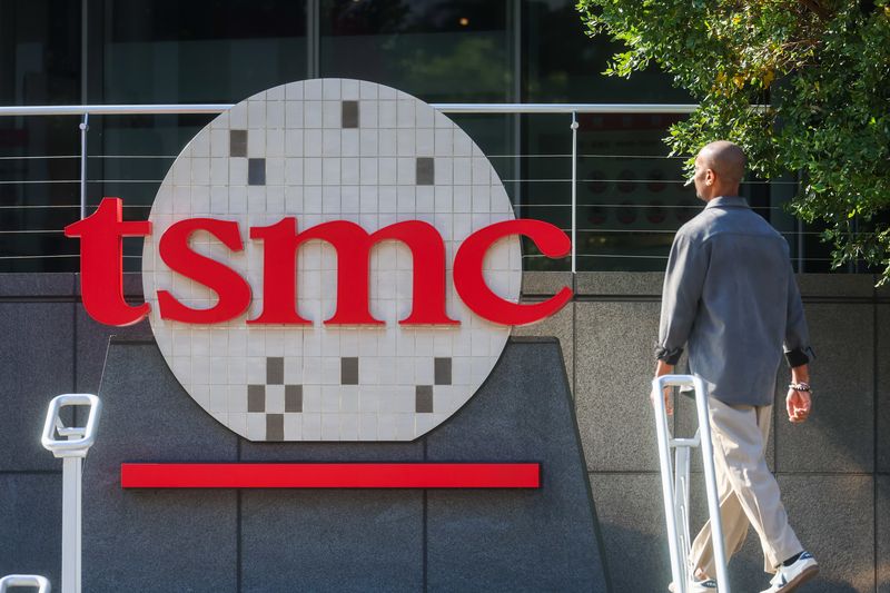
[Financial News] As demand for artificial intelligence (AI) semiconductors surges, TSMC, the world’s No. 1 foundry company, is aggressively expanding semiconductor packaging, another key pillar of AI chip mass production. The company has effectively doubled its advanced semiconductor packaging capacity every year over the past three years, but it is still unable to fully keep up with customer demand.
As competition in AI semiconductors broadens into a full-scale contest spanning advanced process technology, high-bandwidth memory (HBM), and semiconductor packaging, Samsung Electronics is also working to strengthen its advanced packaging capabilities. At the same time, it is seeking to win customers by leveraging its business structure, which includes both foundry and memory operations. The company is also accelerating its push to catch up with TSMC by expanding 2-nanometer mass production capacity at its Taylor, Texas plant.■ Even 10 plants are not enough... TSMC’s sprintAccording to local media in Taiwan on the 14th, Jun He, vice president of TSMC’s advanced packaging technology and service division, said at the recent OCP APAC Summit 2026 in Taipei that the company had doubled production capacity for Chip on Wafer on Substrate (CoWoS), its advanced semiconductor packaging technology, every year over the past three years. He explained that although TSMC now operates 10 advanced packaging plants, it still cannot fully absorb the rapidly growing demand for AI semiconductors.
TSMC is pouring resources into expanding CoWoS capacity because advanced packaging is becoming increasingly important in the AI semiconductor market. CoWoS is TSMC’s advanced packaging process that stacks Graphics Processing Unit (GPU) and high-bandwidth memory (HBM) chips on a single substrate to boost performance while saving space and reducing power consumption. As AI semiconductors become larger and more powerful, and as the amount of HBM connected to GPUs increases, advanced packaging technology that efficiently links multiple chips is emerging as a key factor in AI chip competitiveness, alongside fine process technology. TSMC is also improving its mass-production competitiveness, not just its capacity. Yields for many AI customer products have steadily exceeded 98%, and some products are reportedly reaching 99%.■ Samsung Electronics makes its move in Taylor, TexasSamsung Electronics is also strengthening its advanced packaging competitiveness. The company is refining its 2.5D packaging solution, I-Cube, and its 3D solution, X-Cube. Its recent expanded cooperation with Broadcom Inc. is an extension of that strategy. Samsung Electronics plans to supply memory solutions, including HBM, for Broadcom’s next-generation AI accelerators, while also broadening cooperation to include sub-2-nanometer foundry processes and 2.3D and 2.5D advanced packaging based on those processes. The company is expanding the scope of cooperation beyond HBM supply to include both advanced process technology and advanced packaging.
Along with advanced packaging, Samsung Electronics is also expanding capacity for sub-2-nanometer advanced processes. Ahead of the full-scale launch of its foundry plant in Taylor, Texas, the company is sending key personnel from its Device Solutions Division to the site one after another, speeding up the buildout of a 2-nanometer mass-production system. In April, it dispatched teams and staff responsible for core production functions such as process management, yield verification, and quality response. Additional mass-production personnel are also scheduled to move to the United States in September.
Samsung Electronics is preparing Taylor Plant 1 in the United States, which is set to become a key base for its foundry business, with the goal of starting operations this year. Taylor Plant 2 is planned to break ground by the end of this year, with mass production targeted for 2030. As customer inquiries about the 1.4-nanometer process have recently increased, the company is also considering securing additional fabs.
[email protected] Im Subin, Jeong Won-il Reporter