Samsung Electronics and SK hynix Draw Attention in U.S. This Week as They Face Off Over 'Post-HBM' Roadmaps
- Input
- 2026-08-04 16:54:35
- Updated
- 2026-08-04 16:54:35

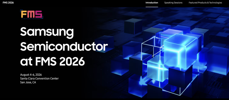
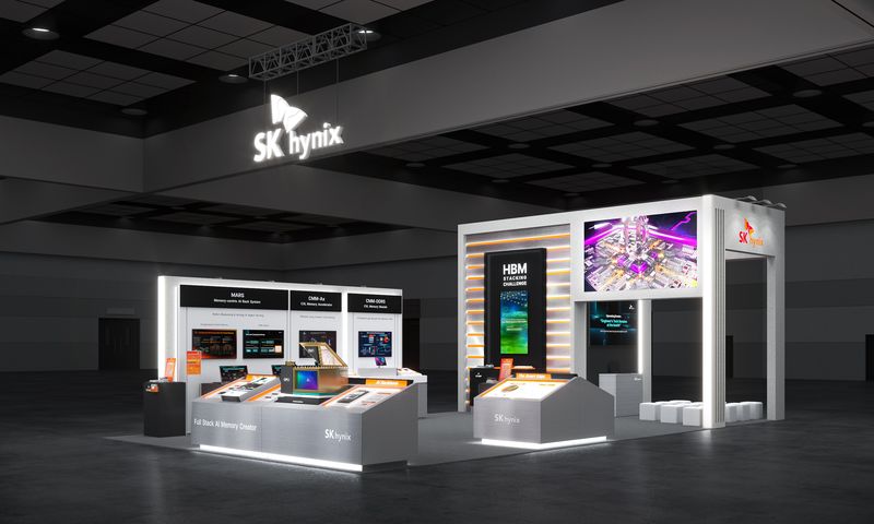
[Financial News] Samsung Electronics and SK hynix are set to compete in the United States with their next-generation artificial intelligence (AI) memory technology roadmaps. The two companies plan to showcase a range of next-generation memory technologies designed to remove bottlenecks in the processing, transfer and storage of data, which are growing rapidly as AI advances.■ Samsung to unveil its 'memory 3D innovation' strategyAccording to the semiconductor industry on the 4th, Samsung Electronics and SK hynix will take part in FMS 2026, held from that day through the 6th local time at the Santa Clara Convention Center in California. Executives from both companies are expected to engage in a tense battle for leadership in the global memory market as they deliver keynote speeches and unveil next-generation memory strategies aimed at easing AI data bottlenecks. FMS marks its 20th anniversary this year and is the world's largest event dedicated to memory and storage.
To coincide with the opening of FMS 2026, SK hynix and SanDisk Corporation jointly unveiled the first standard specification for High Bandwidth Flash (HBF), a next-generation storage technology.
Samsung Electronics will have Vice President Lee Jin-yeop, head of the Flash Development Office in the Memory Business Division, and Executive Director Kim Kyung-ryun of the DRAM Design Team deliver a presentation under the theme of '3D Innovation in Memory and Storage Architecture.' The focus is on a 'memory-centric AI architecture' that uses next-generation High Bandwidth Memory, V-NAND and future memory technologies to resolve AI data bottlenecks.
Industry watchers believe that, because flash and DRAM development executives will present together, Samsung Electronics is likely to outline its next-generation memory structure and roadmap, including 3D DRAM. Unlike HBM, which vertically stacks completed DRAM chips, 3D DRAM is a technology that gives the cells and transistors inside the chip a three-dimensional structure. It is seen as an alternative to overcome the physical limits of planar miniaturization.
In February, Samsung Electronics introduced 'zHBM' as a next-generation memory technology that vertically stacks and connects Graphics Processing Unit (GPU) and High Bandwidth Memory in a 3D structure. At the time, Song Jae-hyuk, Chief Technology Officer (CTO) of Samsung Electronics, said of zHBM, "We expect it to achieve another major breakthrough in bandwidth and power efficiency needed in the era of Physical AI."
HBF is a new memory layer positioned between High Bandwidth Memory and a solid-state drive (SSD). Like HBM, it can transfer data at high speed, while its NAND-based design allows for much greater capacity. As AI inference spreads and the amount of data to be handled rises sharply, it is drawing attention as a technology that can deliver both bandwidth and scalability.
During the event, SK hynix plans to unveil for the first time the wafer and product for its 10th-generation (V10) 375-layer 4D NAND. The 375-layer 4D NAND is notable for delivering 2.5 times better performance per watt than the previous generation, making it well suited for AI infrastructure environments such as data centers that demand both power efficiency and performance. The company plans to begin mass production of high-performance, high-capacity eSSD products based on this technology early next year, further strengthening its NAND leadership in the AI market.
Kim said, "As AI adoption spreads rapidly, this is a point at which the entire data processing structure needs to be redesigned." He added, "Through HBF, we will help expand the boundary between memory and storage and contribute to building a new architecture that improves the efficiency of the entire system."
[email protected] Jung Won-il Reporter