Samsung Electronics Says It Will Apply a GAA-Based 2-Nanometer Process to HBM5, Raising Performance by 50%
- Input
- 2026-07-27 16:11:16
- Updated
- 2026-07-27 16:11:16

Koo Ja-heum, head of technology development at Samsung Electronics Foundry Business and vice president, said on the 27th that "HBM5 is expected to require about 50% higher operating speed than the previous generation, HBM4E." He added, "For the base die, which is the control chip at the bottom of HBM, we are preparing an advanced process that can deliver major improvements in both performance and power efficiency." Koo said, "The base die for HBM5 will use a 2-nanometer process with a GAA structure and implement higher-density through-silicon vias (TSVs)." He emphasized, "By introducing the 2-nanometer process early in HBM5, we will strengthen our technology leadership."
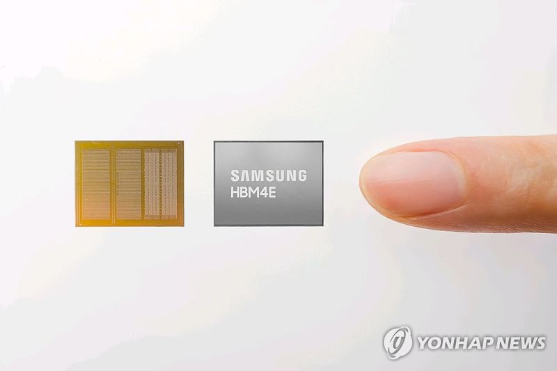
HBM is a product in which core dies, the DRAM chips that store actual data, are stacked and connected on top of a base die. Samsung Electronics manufactures the core dies in memory and the base dies in foundry, then packages them into finished products as part of its turnkey solution. Koo said, "Because Samsung Electronics handles design, manufacturing and packaging, related teams in memory and foundry can collaborate from the design stage to optimize for speed, power, heat and yield." He added, "This also shortens the time needed to complete mass-produced products, which is advantageous from a cost perspective." He went on to say, "Demand for Samsung Foundry's advanced processes is expanding beyond mobile devices." He noted, "Last year, we proved our process competitiveness by winning a 2-nanometer automotive order from Tesla, and since then we have continued to secure orders from major customers such as AI, HPC and CSP companies." Samsung Electronics signed a strategic cooperation memorandum of understanding with Broadcom Inc. in Silicon Valley on the 25th local time for semiconductors worth a total of $200 billion over five years. Large-scale order negotiations are now under way, covering not only memory but also foundry and packaging.
[email protected] Jo Eun-hyo[email protected] Jo Eun-hyo Reporter