Samsung Electronics Says "Advanced Packaging Is the Key in the AI Era" ... Shines a Light on the Future at Nano Korea
- Input
- 2026-07-09 16:24:26
- Updated
- 2026-07-09 16:24:26
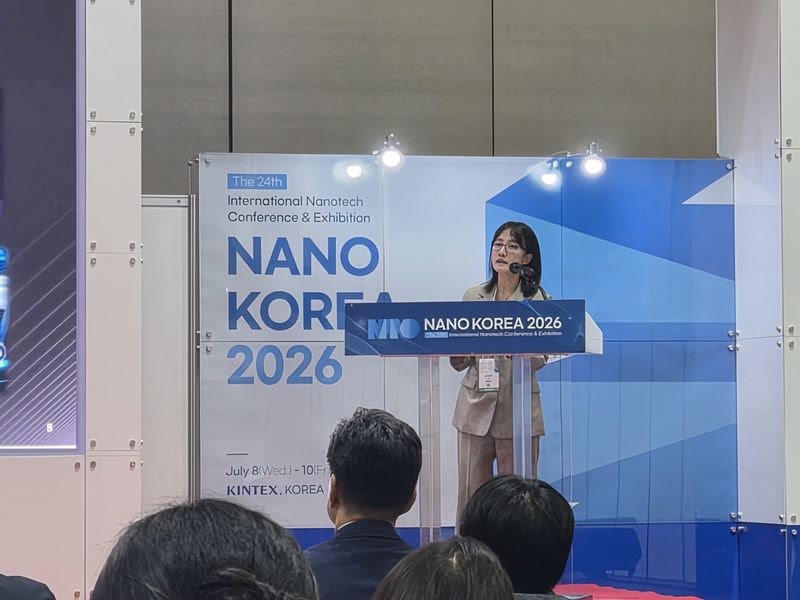
[Financial News, Goyang (Gyeonggi) = Lee Dong-hyuk] "The key driving force in the AI era is advanced packaging."
At the NanoBiz Forum held that day at Nano Korea 2026, the country's largest nanotechnology convergence exhibition at KINTEX in Goyang, Gyeonggi Province, Samsung Electronics Senior Vice President Choi Won-kyung made the remark while giving a presentation on "Semiconductor Packaging Technology in the AI Era."
Choi said Samsung had held close discussions with companies at the forum, listened to the challenges facing the semiconductor industry, and reviewed ways the government could provide support. He stressed that "AI is rapidly spreading beyond data centers into smartphones, home appliances and automobiles, becoming an infrastructure as essential as air and water," adding that "to realize next-generation AI, advanced packaging technology is essential not only for semiconductor performance but also for reducing power consumption and data bottlenecks across the entire system."
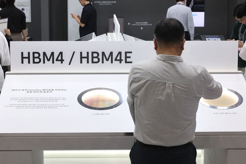
Samsung Electronics is accelerating the advancement of advanced packaging technologies, including High Bandwidth Memory (HBM), 3D logic, silicon photonics, and system-in-package (SiP), to strengthen its competitiveness in AI semiconductors. As AI services expand, power efficiency, heat generation and data transmission speed are becoming decisive factors in semiconductor competitiveness, and packaging is emerging as a core technology that determines system performance rather than merely a back-end process.
In the HBM segment in particular, the company is pushing ahead with the development of hybrid bonding, a next-generation joining technology that increases inter-chip connection density while further refining existing stacking technologies. Through this, Samsung aims to realize next-generation HBM with lower heat generation and higher performance.
Choi explained that "for hybrid bonding to be commercialized, it is important to minimize microscopic foreign particles and precisely control substrate warpage that occurs during the stacking of multiple chips," adding that "this will allow us to secure both quality and yield at the same time."
Samsung Electronics is also pursuing customized HBM development for clients. Its strategy is to achieve low power consumption, high performance and large capacity at the same time by enhancing memory controller functions or changing the memory architecture.
In the logic semiconductor sector, Samsung is expanding development of 3D technology that stacks chips vertically beyond flat structures. It also plans to broaden the use of silicon photonics, which transmits large volumes of data with light instead of electricity in AI data centers, starting with cloud data centers and extending to graphics processing unit (GPU) network equipment.
As competition in AI semiconductors intensifies, power efficiency and heat management are also emerging as key challenges. Samsung said it is developing products by analyzing power consumption and heat generation through server-level simulations from the earliest stages of design, while optimizing chip structures and package materials together.
Choi said, "The core of AI data centers is system technology co-optimization (STCO)," adding that "our goal is to provide AI solutions by optimizing HBM, logic, photonic semiconductors and system-in-package as one system." He continued, "Advanced packaging is not a technology Samsung can develop alone," and said the company would expand its technology ecosystem by working with a wide range of partners, including electronic design automation (EDA) companies, OSAT firms and substrate makers.
Meanwhile, Hwang Kyung-soon, vice president of Samsung Electronics, who delivered the opening remarks at the forum, said that "demand for high-performance, high-efficiency semiconductors is rising rapidly as the AI industry grows," adding that "technological innovation across the semiconductor industry, including memory processes, materials and advanced packaging, is becoming even more important."
[email protected] Lee Dong-hyuk Reporter