Samsung Electronics says 1.4-nanometer process is on track for mass production in 2029
- Input
- 2026-07-01 14:48:54
- Updated
- 2026-07-01 14:48:54
[Financial News] On the 1st, Samsung Electronics unveiled a wide range of next-generation foundry technology strategies, including its 2-nanometer process and design-technology co-optimization (DTCO),
and said its cutting-edge 1.4-nanometer process (SF1.4) is also being developed smoothly, with mass production targeted for 2029.
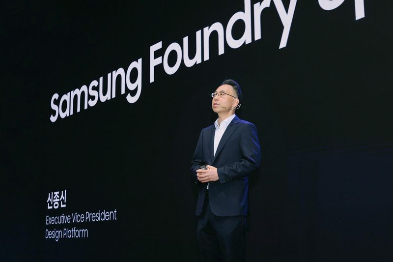
Samsung Electronics held SAFE Forum 2026 at its Seocho headquarters in Seocho-gu, Seoul, and emphasized that it aims to become "the central link in the artificial intelligence (AI) industry." The company said it wants to strengthen its role as a platform for South Korea's system semiconductor industry.
In his keynote speech, Shin Jong-shin, head of the Design Platform Development Office in Samsung Electronics Foundry Business, said, "We are accelerating cooperation with global AI and high-performance computing (HPC) customers while also strengthening collaboration with domestic system semiconductor clients." He added, "Beyond foundry production, we will reinforce our role as a platform for the domestic system semiconductor industry." Shin also said, "Our most advanced 1.4-nanometer process (SF1.4) is being developed smoothly with mass production targeted for 2029, and the enhanced node SF1.4 Plus, which improves yield and performance further, is scheduled to debut in 2030." The 2-nanometer process, which is in high market demand, will also transition to the performance-improved SF2P Plus between 2027 and 2028, before evolving into the follow-up process SF2X. SF2X is a next-generation process that maintains IP compatibility with SF2P and SF2P Plus.
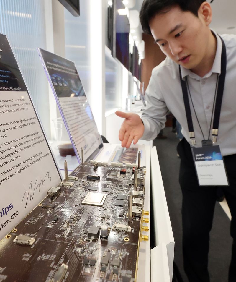
More than 400 people from customer and partner companies attended the event. Twenty-one companies in the fields of electronic design automation (EDA), intellectual property (IP), digital signal processor (DSP), virtual design partner (VDP), and advanced packaging (MDI) set up booths and introduced solutions that support Samsung Electronics foundry customers.
AI fabless company Rebellions and EDA company Siemens EDA also took part as speakers. The two companies presented examples of AI semiconductor development using Samsung Electronics foundry processes and ways to support 2.5D and 3D chip design. Rebellions CEO Seong-hyun Park said, "We developed the 'Rebel 100' neural processing unit (NPU) based on Samsung Electronics' 4-nanometer foundry process and advanced packaging technologies." He added, "Going forward, we will collaborate in the AI semiconductor sector and build sovereign AI." Sovereign AI refers to a strategy aimed at reducing dependence on the technology of specific countries or companies and securing control over domestic data and algorithms.
Jean-Marie Brunet, senior vice president at Siemens EDA, said, "In 2.5D and 3D heterogeneous chip integration, broad support in yield, design verification, reliability, and packaging is essential." He added, "Siemens EDA will help customers rapidly implement AI and HPC semiconductors using Samsung's leading-edge processes."
ehcho@fnnews.com Jo Eun-hyo Reporter