Toward Samsung and SK hynix in Yongin: Semiconductor Materials, Parts, and Equipment Firms Accelerate Move
- Input
- 2026-04-15 18:13:50
- Updated
- 2026-04-15 18:13:50
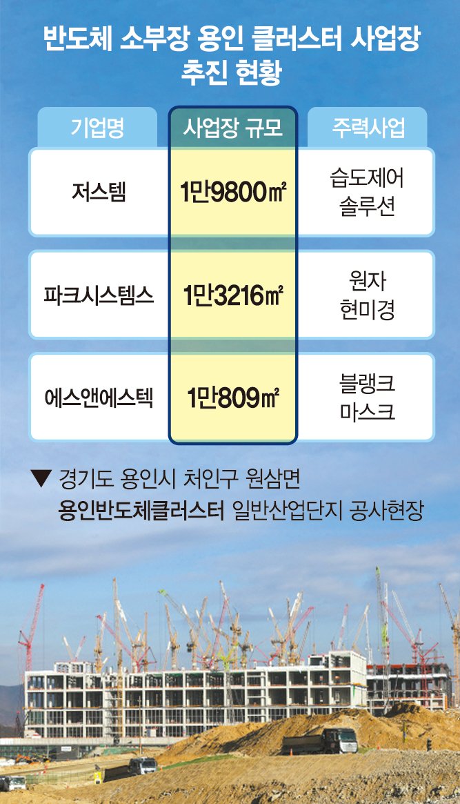
According to industry sources on the 15th, Justem has decided to build a new headquarters with a total floor area of 19,800 square meters inside the Yongin Semiconductor Cluster by 2028. Justem commands more than 80% of the global semiconductor humidity-control solution market with its first-generation solution, N2 Purge. The company has since unveiled its second-generation Justem Flow Strength (JFS) and third-generation Justem Dry Module (JDM), and is accelerating efforts to capture additional market share.
Justem is expanding its equipment business beyond semiconductor humidity-control solutions into a range of fields, including high-vacuum ionizer equipment for OLEDs and roll-to-roll equipment for secondary batteries. A Justem representative said, "We are currently operating Plant 1 in Yongin and Plant 2 in Hwaseong, Gyeonggi Province, with a combined total floor area of 9,900 square meters," adding, "We decided to build a new headquarters in the Yongin Semiconductor Cluster to handle the expected increase in semiconductor humidity-control solution volumes and to prepare for orders of display and secondary-battery equipment."
Park Systems has secured a 13,216-square-meter site in the Yongin Semiconductor Cluster and is coordinating the timing for the start of construction. Park Systems remains the global leader in the Atomic Force Microscope (AFM) market. As semiconductor circuit line widths shrink to the nanometer scale (nm, one-billionth of a meter), AFMs are increasingly used as metrology tools to detect defects in semiconductor devices.
In March, Park Systems completed a new headquarters building with a total floor area of 27,052 square meters on a knowledge-based industrial site in Gwacheon Knowledge Information Town in Gyeonggi Province. The company plans to use the expanded production capacity at this new facility to respond to short-term AFM order volumes.
Earlier, S&S Tech completed an EUV-dedicated center with a total floor area of 10,809 square meters in the Yongin Semiconductor Cluster and has begun mass production there. Through the Yongin center, S&S Tech manufactures semiconductor materials such as EUV blank masks and pellicles, which it supplies to leading domestic chipmakers. Until recently, Korea relied entirely on imports from countries such as Japan for EUV blank masks.
Industry observers say the move by semiconductor materials, parts, and equipment companies into the Yongin Semiconductor Cluster reflects the government's strategy to foster Yongin as a core national semiconductor hub. The Yongin Semiconductor Cluster is a mega-scale national project that will see more than 300 trillion won invested by 2042.
An industry official noted, "With the advent of the artificial intelligence (AI) era, demand for semiconductors is surging, driven by accelerators and High Bandwidth Memory (HBM) used in AI data centers," and continued, "In response, Samsung Electronics has committed to investments in Pyeongtaek, Gyeonggi Province, and SK hynix in Cheongju, North Chungcheong Province, and both have now confirmed investments in the Yongin Cluster. To provide close support to these chipmakers, semiconductor materials, parts, and equipment companies are steadily moving into Yongin."
butter@fnnews.com Kang Kyung-rae Reporter