Samsung Foundry Spreads Its Wings Again, Poised to Return to Profit This Year
- Input
- 2026-03-11 18:14:08
- Updated
- 2026-03-11 18:14:08
■ Foundry division triples its customer base
According to the semiconductor industry on the 11th, Samsung Electronics’ foundry division had 121 customers as of the end of last year, more than tripling from 35 in 2017.
Samsung Electronics aims to make 2027 the first year of full-fledged growth for its foundry business. The company plans to rapidly expand its customer base in areas that require advanced process technologies, such as AI accelerators, data center chips and autonomous driving processors. It is currently working with Tesla, Broadcom, Intel, Cisco Systems (Cisco), Infineon Technologies and Waymo on test chips (MPW) and various collaboration projects. Industry observers note that its customer portfolio has diversified beyond traditional IT clients like Qualcomm and Sony to include next-generation segments such as AI semiconductors, data center chips and autonomous driving chips.
Despite chronic losses over several years, Samsung Electronics has continued to invest in its foundry business. The foundry workforce has grown from about 13,000 employees in 2017 to roughly 21,000 recently. Among them, overseas staff have nearly doubled, from around 3,000 to about 6,000.
The company has also maintained an aggressive investment stance. According to McKinsey & Company, the cost of building a single semiconductor fab has soared from 1.6 billion dollars (about 2.34 trillion won) in 2009 to around 17 billion dollars (about 25 trillion won) in 2022, more than a tenfold increase. This is because process miniaturization requires more complex equipment and larger facilities. Samsung Electronics has invested roughly 17 billion dollars in the foundry plant it is building in Taylor, Texas, in the State of Texas.
■ High Bandwidth Memory, the new cash cow, helps foundry earn proper margins
Recently, the growing demand for High Bandwidth Memory (HBM) has also been viewed as a positive factor for the foundry business. HBM packages for AI accelerators combine not only memory but also logic semiconductors, and this integration is increasing the role of foundry processes. In particular, Samsung has begun supplying the next-generation High Bandwidth Memory 4 (HBM4), the industry’s first to be delivered to Nvidia Corporation, and is applying its 4-nanometer foundry process to the "base die" at the bottom of the HBM4 stack. Analysts say this is creating a virtuous cycle in which the memory boom leads to higher foundry volumes. An internal company source said, "In the past, there was a perception that we were not getting sufficient pricing for foundry services, but as AI demand has grown, we are increasingly able to charge what our work is worth."
Moves by customers to reduce their heavy dependence on Taiwan Semiconductor Manufacturing Company (TSMC), whose production lines are now near full capacity, are also seen as a tailwind. This so-called "TSMC trickle-down effect" is benefiting rivals. Within the industry, some say Samsung Electronics’ foundry, which has taken the lead in introducing a cutting-edge 2-nanometer process, could become one of the few viable alternatives capable of meeting customer requirements.
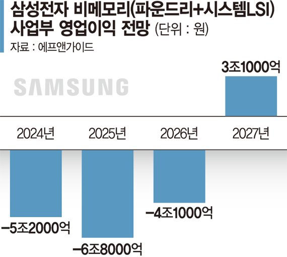
Against this backdrop, there is already a broad internal consensus that the foundry business will turn profitable in the fourth quarter of this year. Although the division has posted losses for years due to weak market conditions and heavy upfront investment, many expect earnings to improve in earnest as demand for AI semiconductors grows and new customer wins start to show up in the numbers. An industry official explained, "Even after a contract is signed, the foundry business structure is such that it takes considerable time before production begins and revenue is recognized," adding, "The customer orders we secured last year are gradually moving into the production phase and will be reflected in this year’s results."
soup@fnnews.com Im Soo-bin, Jung Won-il Reporter