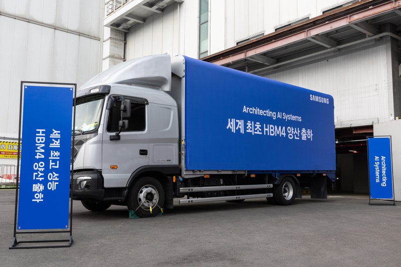
Samsung ships industry’s fastest HBM4, raising the performance ceiling for AI accelerators
- Input
- 2026-02-12 17:01:01
- Updated
- 2026-02-12 17:01:01
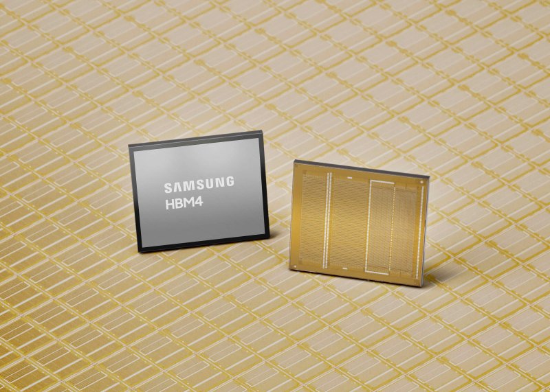
Analysts point to integrated optimization of design and process, combining memory and foundry strengths, as the key reason Samsung Electronics was able to meet stringent customer speed requirements and move ahead with the world’s first mass-production shipments. For HBM4, Samsung stacked 1c DRAM, a 6th-generation 10-nanometer-class node that is one generation ahead of competitors’ 5th-generation products, and used a 4-nanometer foundry process for the base die, implementing a leading-edge technology combination ahead of rivals. This was possible because Samsung is an integrated device manufacturer (IDM) that can provide a one-stop solution from memory to foundry. Being able to coordinate design, manufacturing, and packaging within a single company makes it easier to boost both performance and yield at the same time.
The chip also delivers notable gains in power efficiency. As the number of data-transfer I/O pins doubled from 1,024 to 2,048, Samsung Electronics applied low-power design techniques to the core die to address the resulting increase in power consumption and heat concentration. In addition, by introducing a low-voltage design for data transmission and reception through through-silicon via (TSV) technology and optimizing the power distribution network (PDN), the company improved energy efficiency by about 40% over the previous generation. Thermal resistance characteristics improved by around 10%, and heat dissipation performance by about 30%.
Building on this significant technology lead, Samsung Electronics also unveiled a roadmap for follow-up HBM4 products. Following the first mass-production shipment of HBM4 announced the same day, the company plans to begin sampling HBM4E (High Bandwidth Memory 4E) in the second half of this year. It also stated that custom high-bandwidth memory (custom HBM) will be sampled sequentially from 2027, tailored to the specific requirements of each customer.
■Three-way HBM4 battle to heat up in the first quarterWith Samsung Electronics securing the “world’s first” title, full-scale competition in the HBM4 market is expected to begin in the first quarter of this year. SK hynix, currently the number one player in the HBM market, has remained silent on its exact timing, but plans to maintain its edge based on stable relationships with customers and strong production volumes built up since HBM3E. Some forecasts suggest SK hynix could account for about 70% of NVIDIA’s HBM4 supply. Recently, global credit rating agency S&P commented, "As Samsung Electronics, Micron Technology and other major competitors ramp up production in the high-growth, high-margin HBM chip market, SK hynix’s market share could decline, but its market position is unlikely to weaken significantly for at least the next two to three years."
U.S. memory maker Micron Technology also pushed back strongly, directly rejecting recent speculation that it had been dropped from NVIDIA’s supply chain. The company stated, "We are mass-producing HBM4 and have begun shipping to customers." On the 11th (local time), at a semiconductor conference hosted by U.S. research firm Wolfe Research, Mark Murphy, Micron’s Chief Financial Officer (CFO), described the reports about being excluded from NVIDIA’s supply chain as "inaccurate coverage" and said, "Micron is already accelerating high-volume production of HBM4 and has started shipments to customers." The core customer is widely believed to be NVIDIA.
As Micron mounts an active defense, observers expect the HBM4 market—once thought likely to form a "two-strong" structure—to become even more competitive. From NVIDIA’s perspective, it is more advantageous to foster competition among three suppliers than to rely on a single vendor for HBM4. A semiconductor industry insider noted, "NVIDIA is likely to work closely with all three companies to reduce dependence on any single vendor and secure better pricing power."
soup@fnnews.com Im Soo-bin, Jung Won-il Reporter