Samsung the Technologist Is Back: Riding HBM4 Momentum, It Unveils Roadmap for Next-Generation Custom HBM and zHBM
- Input
- 2026-02-11 12:10:25
- Updated
- 2026-02-11 12:10:25
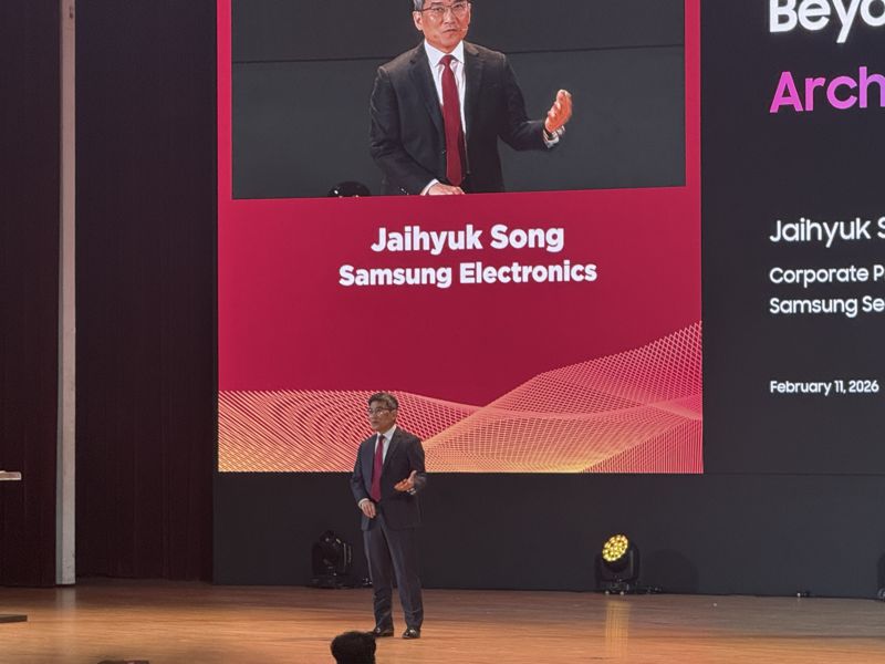
[Financial News] Jaihyuk Song, president and Chief Technology Officer (CTO) of Samsung Electronics' Device Solutions Division (DS),pictured,said on the 11th, "Samsung has the advantage of possessing both foundry and dynamic random-access memory (DRAM) capabilities, and as a result we are receiving positive feedback from customers, including Nvidia, on the bandwidth and energy efficiency of our high-bandwidth memory (HBM4)."
Song was the first keynote speaker at Semicon Korea 2026, the country’s largest semiconductor exhibition, held at COEX in Seoul, where he highlighted these points while introducing Samsung’s HBM4 products. Before the event, he also told reporters, regarding the industry’s first mass production of HBM4, "We are once again able to show Samsung responding to what customers want with the best technology in the world." Samsung Electronics’ HBM4 is regarded as being at a world-leading level that surpasses the standards of the Joint Electron Device Engineering Council (JEDEC). By simultaneously applying 1c DRAM (6th-generation 10-nanometer class) and a 4-nanometer foundry process, it achieved up to 11.7 gigabits per second (Gbps).
Artificial intelligence (AI) is evolving beyond traditional speech- and language-recognition systems into agentic AI that performs specific tasks, and further into physical AI that perceives and acts in the real world. This evolution is inevitably driving an explosive increase in data throughput and workloads. That is why AI accelerator companies need next-generation products such as HBM4.
Song noted, "Inference currently accounts for about 70% of total AI workloads, but training and data-centric workloads are also growing exponentially." He added, "As we enter the digital AI phase, this workload growth is expected to accelerate even further, and accordingly, demand for memory bandwidth and capacity is surging."
In line with these trends, Samsung Electronics’ Device Solutions Division says it is also preparing next-generation memory products. Beyond standard HBM, the company is developing custom high-bandwidth memory (custom HBM, or cHBM) tailored to individual customers. "We are preparing custom HBM that secures much higher bandwidth by proactively adopting die-to-die interface intellectual property (IP)," Song explained, adding, "We have obtained experimental results showing that we can cut the number of I/O pins while reducing power consumption by half."
Samsung is also working on zHBM, which extends HBM—where DRAM chips are stacked vertically—to a new level. "For zHBM, we are preparing an architecture that expands along the Z-axis," Song said, emphasizing that "zHBM is expected to deliver major breakthroughs in bandwidth and power efficiency required in the era of physical AI." The company has additionally secured hybrid bonding (HCB) technology, regarded as a next-generation packaging solution. According to Samsung, applying HCB reduces thermal resistance by 20% and lowers the base die temperature by 11% compared with existing technologies.
soup@fnnews.com Im Subin and Jeong Won-il Reporter