DB HiTek Secures 650V GaN HEMT Process... 'Targeting AI Data Center Market'
- Input
- 2025-09-11 09:55:13
- Updated
- 2025-09-11 09:55:13
Customer support officially begins, MPW available at the end of October
[Financial News] Specialized foundry (semiconductor contract manufacturing) company DB HiTek has completed the development of the next-generation power semiconductor 650V E-Mode GaN HEMT (Enhancement-mode Gallium Nitride High Electron Mobility Transistor) process and announced on the 11th that it will provide a GaN dedicated Multi-Project Wafer (MPW) for customers to trial-produce products by the end of next month.
Semiconductors made from GaN material are stronger against high voltage, high frequency, and high temperature compared to existing silicon (Si)-based semiconductors, and have higher power efficiency, making them popular as next-generation power semiconductors along with silicon carbide (SiC). In particular, demand is rapidly increasing in new high-growth areas such as electric vehicles, artificial intelligence (AI) data centers, fast charging, 5G, and robots.
The 650V E-Mode GaN HEMT developed by DB HiTek this time is characterized by high-speed switching and stability, making it highly useful in electric vehicle chargers, data center power converters, and 5G communication fields.
DB HiTek has been developing processes for compound semiconductors such as GaN and SiC as next-generation businesses since 2022 when the market was in its early stages. A DB HiTek representative said, "We have already been recognized for our global technological competitiveness in Si-based power semiconductors by developing the world's first 0.18um composite voltage device (BCDMOS), and with the addition of the GaN process, the company's competitiveness as a power semiconductor foundry company is expected to be further strengthened."
Starting with the development of this 650V GaN HEMT process, DB HiTek plans to sequentially develop a 200V GaN process and a 650V GaN process that can be designed in the form of an integrated circuit (IC) by the end of 2026. After that, they plan to solidify their business foundation by expanding the process to a wider voltage range, considering market conditions and customer demand.
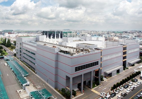
In line with this, DB HiTek is also promoting the expansion of cleanrooms at the Sangwoo Campus in Eumseong, Chungbuk. According to the company, the new cleanroom will be able to expand production by about 35,000 8-inch wafers per month, and GaN, BCDMOS, SiC, etc., are expected to be produced. Once the expansion is completed, DB HiTek's production capacity will increase by 23% from the current 154,000 to 190,000 wafers.
Meanwhile, to promote and strengthen the SiC technology currently under development, DB HiTek will participate in the International Conference on Silicon Carbide and Related Materials (ICSCRM) 2025, held at BEXCO in Busan from the 15th to the 18th. At this event, DB HiTek will showcase the latest technology development status of power semiconductors, including SiC, GaN, and BCDMOS, and meet with customers and industry officials.
soup@fnnews.com Lim Subin Reporter